LT1996
1
1996f
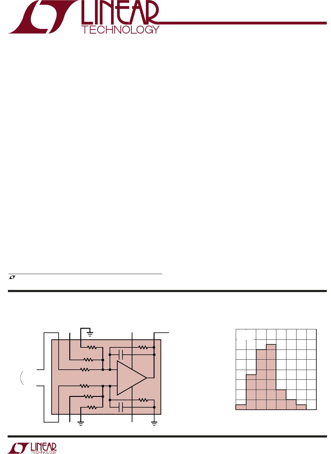
RESISTOR MATCHING (%)
PERCENTAGE OF UNITS (%)
0.04
1996 TA01b
0.02
0
0.02
40
35
30
25
20
15
10
5
0
0.04
LT1996A
G = 81
TYPICAL APPLICATIO
U
FEATURES
Pin Configurable as a Difference Amplifier,
Inverting and Noninverting Amplifier
Difference Amplifier
Gain Range 9 to 117
CMRR >80dB
Noninverting Amplifier
Gain Range 0.008 to 118
Inverting Amplifier
Gain Range –0.08 to –117
Gain Error: <0.05%
Gain Drift: < 3ppm/°C
Wide Supply Range: Single 2.7V to Split ±18V
Micropower Operation: 100µA Supply
Input Offset Voltage: 50µV (Max)
Gain Bandwidth Product: 560kHz
Rail-to-Rail Output
Space Saving 10-Lead MSOP and DFN Packages
Precision, 100µA
Gain Selectable Amplifier
The LT
®
1996 combines a precision operational amplifier
with eight precision resistors to form a one-chip solution
for accurately amplifying voltages. Gains from –117 to
118 with a gain accuracy of 0.05% can be achieved without
any external components. The device is particularly well
suited for use as a difference amplifier, where the excellent
resistor matching results in a common mode rejection
ratio of greater than 80dB.
The amplifier features a 50µV maximum input offset
voltage and a gain bandwidth product of 560kHz. The
device operates from any supply voltage from 2.7V to 36V
and draws only 100µA supply current on a 5V supply. The
output swings to within 40mV of either supply rail.
The internal resistors have excellent matching character-
istics; variation is 0.05% over temperature with a guaran-
teed matching temperature coefficent of less than 3ppm/°C.
The resistors are also extremely stable over voltage,
exhibiting a nonlinearity of less than 10ppm.
The LT1996 is fully specified at 5V and ±15V supplies and
from –40°C to 85°C. The device is available in space
saving 10-lead MSOP and DFN packages. For an amplifier
with selectable gains from –13 to 14, see the LT1991 data
sheet.
DESCRIPTIO
U
APPLICATIO S
U
Rail-to-Rail Gain = 9 Difference Amplifier Distribution of Resistor Matching
+
15V
–15V
V
IN
V
M(IN)
V
P(IN)
+
V
OUT
= V
REF
+ 9 •
V
IN
SWING 40mV TO
EITHER RAIL
INPUT RANGE
±60V
R
IN
= 100k
LT1996
1996 TA01
450k/81
450k/81
450k/27
450k/27
450k/9
450k
450k
450k/9
4pF
4pF
V
REF
, LTC and LT are registered trademarks of Linear Technology Corporation.
All other trademarks are the property of their respective owners. Patents Pending.
Handheld Instrumentation
Medical Instrumentation
Strain Gauge Amplifiers
Differential to Single-Ended Conversion
LT1996
2
1996f
SYMBOL PARAMETER CONDITIONS MIN TYP MAX UNITS
G Gain Error V
S
= ±15V, V
OUT
= ±10V; R
L
= 10k
G = 81; LT1996AMS
±0.02 ±0.05 %
G = 27; LT1996AMS
±0.03 ±0.06 %
G = 9; LT1996AMS
±0.03 ±0.07 %
G = 81; LT1996ADD ±0.02 ±0.05 %
G = 27; LT1996ADD
±0.02 ±0.07 %
G = 9; LT1996ADD
±0.03 ±0.08 %
G = 81; LT1996 ±0.04 ±0.12 %
G = 27; LT1996
±0.04 ±0.12 %
G = 9; LT1996
±0.04 ±0.12 %
GNL Gain Nonlinearity V
S
= ±15V; V
OUT
= ±10V; R
L
= 10k; G = 9 1 10 ppm
G/T Gain Drift vs Temperature (Note 6) V
S
= ±15V; V
OUT
= ±10V; R
L
= 10k 0.3 3 ppm/°C
CMRR Common Mode Rejection Ratio, V
S
= ±15V; G = 9; V
CM
= ±15.3V
Referred to Inputs (RTI) LT1996AMS
80 100 dB
LT1996ADD
80 100 dB
LT1996
70 100 dB
V
S
= ±15V; G = 27; V
CM
= –14.5V to 14.3V
LT1996AMS
95 105 dB
LT1996ADD
90 105 dB
LT1996
75 105 dB
PACKAGE/ORDER I FOR ATIO
UUW
Total Supply Voltage (V
+
to V
) ............................... 40V
Input Voltage (Pins P9/M9, Note 2) ....................... ±60V
Input Current
(Pins P27/M27/P81/M81, Note 2) .................. ±10mA
Output Short-Circuit Duration (Note 3) ............ Indefinite
Operating Temperature Range (Note 4) ...40°C to 85°C
Specified Temperature Range (Note 5) ....40°C to 85°C
ORDER PART
NUMBER
MS PART MARKING*T
JMAX
= 150°C, θ
JA
= 230°C/W
LTBPB
LT1996CMS
LT1996IMS
LT1996ACMS
LT1996AIMS
ABSOLUTE AXI U RATI GS
W
WW
U
(Note 1)
The
denotes the specifications which apply over the full operating
temperature range, otherwise specifications are at T
A
= 25°C. Difference amplifier configuration, V
S
= 5V, 0V or ±15V;
V
CM
= V
REF
= half supply, unless otherwise noted.
*Temperature and electrical grades are identified by a label on the shipping container. Consult LTC Marketing for parts specified with wider operating temperature ranges.
1
2
3
4
5
P9
P27
P81
V
EE
REF
10
9
8
7
6
M9
M27
M81
V
CC
OUT
TOP VIEW
MS PACKAGE
10-LEAD PLASTIC MSOP
Maximum Junction Temperature
DD Package ...................................................... 125°C
MS Package ..................................................... 150°C
Storage Temperature Range
DD Package .......................................65°C to 125°C
MS Package ......................................65°C to 150°C
MSOP–Lead Temperature (Soldering, 10 sec)...... 300°C
ORDER PART
NUMBER
DD PART MARKING*
T
JMAX
= 125°C, θ
JA
= 160°C/W
UNDERSIDE METAL CONNECTED TO V
EE
(PCB CONNECTION OPTIONAL)
LBPC
LT1996CDD
LT1996IDD
LT1996ACDD
LT1996AIDD
TOP VIEW
DD PACKAGE
10-LEAD (3mm × 3mm) PLASTIC DFN
10
9
6
7
8
4
5
3
2
1
M9
M27
M81
V
CC
OUT
P9
P27
P81
V
EE
REF
ELECTRICAL CHARACTERISTICS
LT1996
3
1996f
SYMBOL PARAMETER CONDITIONS MIN TYP MAX UNITS
CMRR Common Mode Rejection Ratio (RTI) V
S
= ±15V; G = 81; V
CM
= –14.1V to 13.9V
LT1996AMS
105 120 dB
LT1996ADD
100 120 dB
LT1996
85 120 dB
V
CM
Input Voltage Range (Note 7) P9/M9 Inputs
V
S
= ±15V; V
REF
= 0V –15.5 15.3 V
V
S
= 5V, 0V; V
REF
= 2.5V 0.84 3.94 V
V
S
= 3V, 0V; V
REF
= 1.25V 0.98 1.86 V
P9/M9 Inputs, P81/M81 Connected to REF
V
S
= ±15V; V
REF
= 0V –60 60 V
V
S
= 5V, 0V; V
REF
= 2.5V –12.6 15.6 V
V
S
= 3V, 0V; V
REF
= 1.25V –1.25 6.8 V
P27/M27 Inputs
V
S
= ±15V; V
REF
= 0V –14.5 14.3 V
V
S
= 5V, 0V; V
REF
= 2.5V 0.95 3.84 V
V
S
= 3V, 0V; V
REF
= 1.25V 1 1.82 V
P81/M81 Inputs
V
S
= ±15V; V
REF
= 0V –14.1 13.9 V
V
S
= 5V, 0V; V
REF
= 2.5V 0.99 3.81 V
V
S
= 3V, 0V; V
REF
= 1.25V 1 1.8 V
V
OS
Op Amp Offset Voltage (Note 8) LT1996AMS, V
S
= 5V, 0V 15 50 µV
135 µV
LT1996AMS, V
S
= ±15V 15 80 µV
160 µV
LT1996MS 25 100 µV
200 µV
LT1996DD 25 150 µV
250 µV
V
OS
/T Op Amp Offset Voltage Drift (Note 6) 0.3 1 µV/°C
I
B
Op Amp Input Bias Current 2.5 5 nA
7.5 nA
I
OS
Op Amp Input Offset Current LT1996A 50 500 pA
750 pA
LT1996 50 1000 pA
1500 pA
Op Amp Input Noise Voltage 0.01Hz to 1Hz 0.35 µV
P-P
0.01Hz to 1Hz 0.07 µV
RMS
0.1Hz to 10Hz 0.25 µV
P-P
0.1Hz to 10Hz 0.05 µV
RMS
e
n
Input Noise Voltage Density G = 9; f = 1kHz 46 nV/Hz
(Includes Resistor Noise) G = 117; f = 1kHz 18 nV/Hz
R
IN
Input Impedance (Note 10) P9 (M9 = Ground) 350 500 650 k
P27 (M27 = Ground)
326.9 467 607.1 k
P81 (M81 = Ground)
319.2 456 592.8 k
M9 (P9 = Ground) 35 50 65 k
M27 (P27 = Ground)
11.69 16.7 21.71 k
M81 (P81 = Ground)
3.85 5.5 7.15 k
The denotes the specifications which apply over the full operating
temperature range, otherwise specifications are at T
A
= 25°C. Difference amplifier configuration, V
S
= 5V, 0V or ±15V;
V
CM
= V
REF
= half supply, unless otherwise noted.
ELECTRICAL CHARACTERISTICS

LT1996ACDD#TRPBF

Mfr. #:
Manufacturer:
Analog Devices Inc.
Description:
Precision Amplifiers Prec, 100 A Gain Sel Amp
Lifecycle:
New from this manufacturer.
Delivery:
DHL FedEx Ups TNT EMS
Payment:
T/T Paypal Visa MoneyGram Western Union