LT1996
10
1996f
Consider Figure 1. This shows the LT1996 configured as
a gain of 117 difference amplifier on a single supply with
Figure 3. Calculating Additional Voltage Range of
Inverting Inputs
These two voltages represent the high and low extremes
of the common mode input range, if the other limits have
not already been exceeded (1 and 3, above). In most cases,
the inverting inputs M9 through M81 can be taken further
than these two extremes because doing this does not
move the op amp input common mode. To calculate the
limit on this additional range, see Figure 3. Note that, with
Figure 1. Difference Amplifier Cannot Produce 0V on a Single
Supply. Provide a Negative Supply, or Raise Pin 5, or Provide
400µV of V
DM
the output REF connected to ground. This is a great circuit,
but it does not support V
DM
= 0V at any common mode
because the output clips into ground while trying to
produce 0V
OUT
. It can be fixed simply by declaring the
valid input differential range not to extend below +0.4mV,
or by elevating the REF pin above 40mV, or by providing
a negative supply.
Calculating Input Voltage Range
Figure 2 shows the LT1996 in the generalized case of a
difference amplifier, with the inputs shorted for the com-
mon mode calculation. The values of R
F
and R
G
are
dictated by how the P inputs and REF pin are connected.
By superposition we can write:
V
INT
= V
EXT
• (R
F
/(R
F
+ R
G
)) + V
REF
• (R
G
/(R
F
+ R
G
))
Or, solving for V
EXT
:
V
EXT
= V
INT
• (1 + R
G
/R
F
) – V
REF
• R
G
/R
F
But valid V
INT
voltages are limited to V
CC
– 1.2V and V
EE
+
1V, so:
MAX V
EXT
= (V
CC
– 1.2) • (1 + R
G
/R
F
) – V
REF
• R
G
/R
F
and:
MIN V
EXT
= (V
EE
+ 1) • (1 + R
G
/R
F
) – V
REF
• R
G
/R
F
Figure 2. Calculating CM Input Voltage Range
V
MORE
= 0, the op amp output is at V
REF
. From the max
V
EXT
(the high cm limit), as V
MORE
goes positive, the op
amp output will go more negative from V
REF
by the amount
V
MORE
• R
F
/R
G
, so:
V
OUT
= V
REF
– V
MORE
• R
F
/R
G
Or:
V
MORE
= (V
REF
– V
OUT
) • R
G
/R
F
The most negative that V
OUT
can go is V
EE
+ 0.04V, so:
Max V
MORE
= (V
REF
– V
EE
– 0.04V) • R
G
/R
F
(should be positive)
The situation where this function is negative, and therefore
problematic, when V
REF
= 0 and V
EE
= 0, has already been
dealt with in Figure 1. The strength of the equation is
demonstrated in that it provides the three solutions
APPLICATIO S I FOR ATIO
WUU
U
4pF
4pF
+
1996 F01
450k/81
450k/27
450k/9
450k/81
450k/27
450k/9
450k
450k
REF
5V
V
CM
2.5V
V
DM
0V
+
8
7
6
5
4
9
10
1
2
3
LT1996
V
OUT
= 117 • V
DM
4pF
4pF
+
V
REF
R
F
R
F
R
G
R
G
1996 F02
V
EXT
V
INT
V
CC
V
EE
+
V
REF
R
F
R
F
R
G
R
G
1996 F03
V
EXT
MAX OR MIN
V
INT
V
MORE
V
CC
V
EE
LT1996
11
1996f
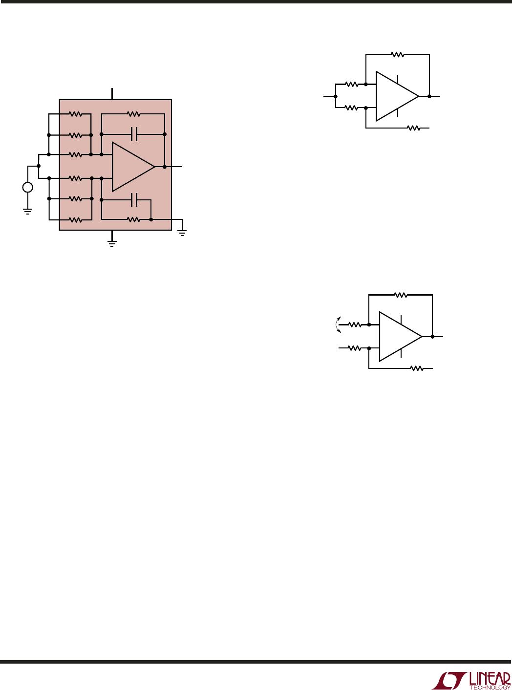
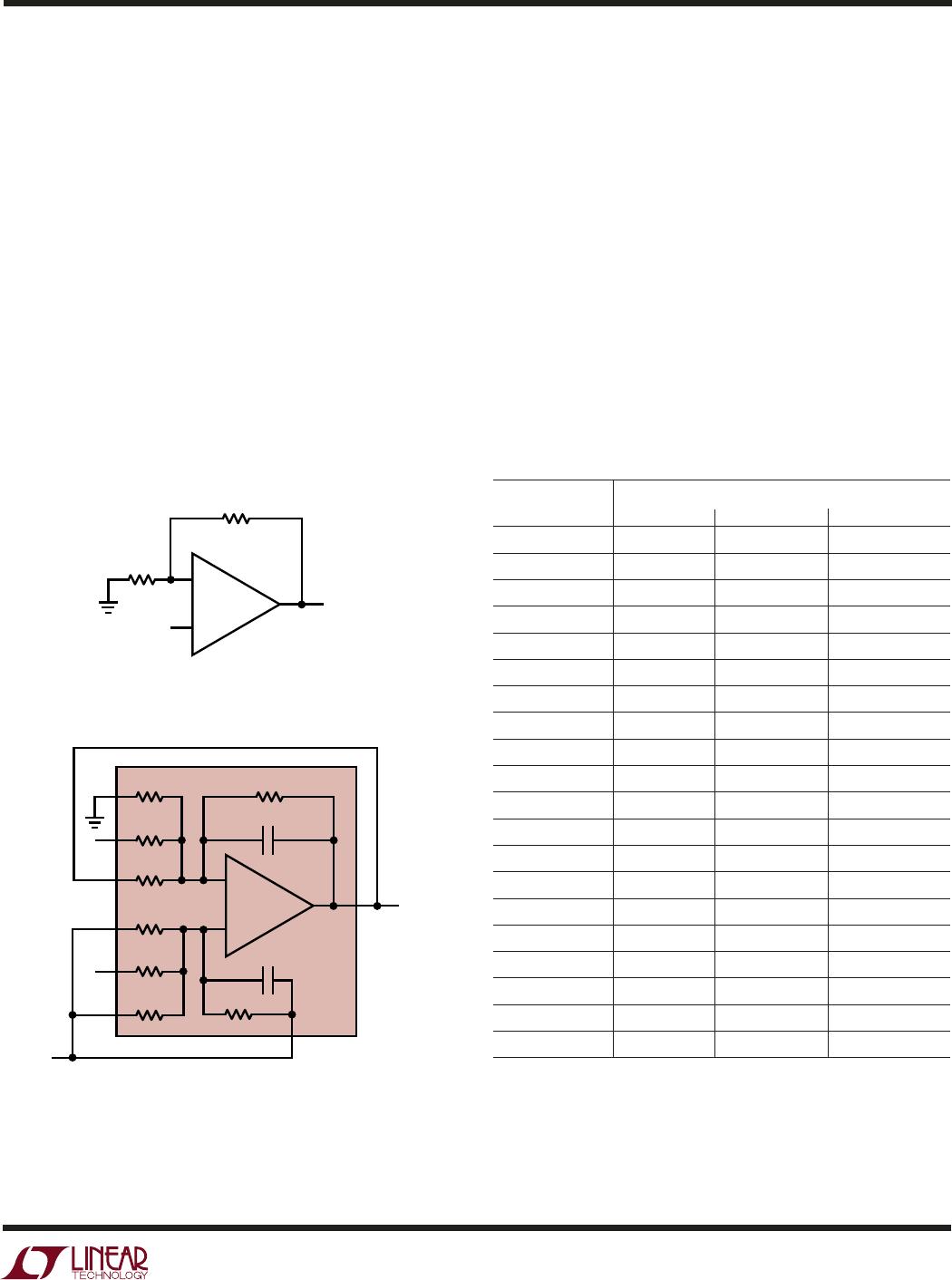
representation of the circuit on the top. The LT1996 is
shown on the bottom configured in a precision gain of 9.1.
One of the benefits of the noninverting op amp configura-
tion is that the input impedance is extremely high. The
LT1996 maintains this benefit. Given the finite number of
available feedback resistors in the LT1996, the number of
gain configurations is also finite. The complete list of such
Hi-Z input noninverting gain configurations is shown in
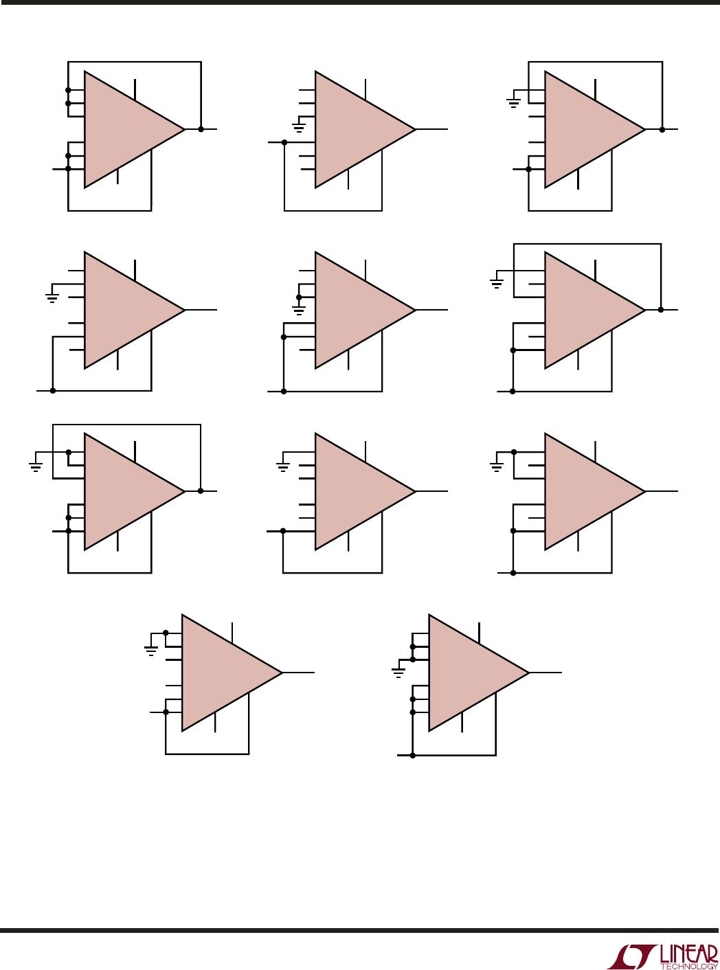
Table 1. Many of these are also represented in Figure 5 in
schematic form. Note that the P-side resistor inputs have
been connected so as to match the source impedance
seen by the internal op amp inputs. Note also that gain and
noise gain are identical, for optimal precision.
Table 1. Configuring the M Pins for Simple Noninverting Gains.
The P Inputs are driven as shown in the examples on the next
page
M81, M27, M9 Connection
Gain M81 M27 M9
1 Output Output Output
1.08 Output Output Grounded
1.11 Output Float Grounded
1.30 Output Grounded Output
1.32 Float Output Grounded
1.33 Output Grounded Float
1.44 Output Grounded Grounded
3.19 Grounded Output Output
3.7 Float Grounded Output
3.89 Grounded Output Float
4.21 Grounded Output Grounded
9.1 Grounded Float Output
10 Float Float Grounded
11.8 Grounded Grounded Output
28 Float Grounded Float
37 Float Grounded Grounded
82 Grounded Float Float
91 Grounded Float Grounded
109 Grounded Grounded Float
118 Grounded Grounded Grounded
suggested in Figure 1: raise V
REF
, lower V
EE
, or provide
some negative V
MORE
.
Likewise, from the lower common mode extreme, making
the negative input more negative will raise the output
voltage, limited by V
CC
– 0.04V.
MIN V
MORE
= (V
REF
– V
CC
+ 0.04V) • R
G
/R
F
(should be negative)
Again, the additional input range calculated here is only
available provided the other remaining constraint is not
violated, the maximum voltage allowed on the pin.
The Classical Noninverting Amplifier: High Input Z
Perhaps the most common op amp configuration is the
noninverting amplifier. Figure 4 shows the textbook
Figure 4. The LT1996 as a Classical Noninverting Op Amp
APPLICATIO S I FOR ATIO
WUU
U
4pF
4pF
+
R
F
R
G
V
IN
V
IN
V
OUT
V
OUT
V
OUT
= GAIN • V
IN
GAIN = 1 + R
F
/R
G
+
1996 F04
450k/81
450k/27
450k/9
450k/81
450k/27
450k/9
450k
450k
8
6
5
9
10
1
2
3
LT1996
CLASSICAL NONINVERTING OP AMP CONFIGURATION.
YOU PROVIDE THE RESISTORS.
CLASSICAL NONINVERTING OP AMP CONFIGURATION
IMPLEMENTED WITH LT1991. R
F
= 45k, R
G
= 5.6k, GAIN = 9.1.
GAIN IS ACHIEVED BY GROUNDING, FLOATING OR FEEDING BACK
THE AVAILABLE RESISTORS TO ARRIVE AT DESIRED R
F
AND R
G
.
WE PROVIDE YOU WITH <0.1% RESISTORS.
4pF
4pF
LT1996
12
1996f
Figure 5. Some Implementations of Classical Noninverting
Gains Using the LT1996. High Input Z Is Maintained
APPLICATIO S I FOR ATIO
WUU
U
V
S
V
S
V
S
+
1996 F05
M81
M27
M9
P9
P27
P81
OUT
V
CC
V
OUT
V
IN
V
EE
V
S
+
V
S
V
S
+
V
S
V
S
+
V
S
V
S
+
V
S
V
S
+
V
S
V
S
+
V
S
V
S
+
V
S
V
S
+
V
S
V
S
+
V
S
V
S
+
REF
LT1996
8
9
10
1
2
3
7
6
5
4
M81
M27
M9
P9
P27
P81
OUT
V
CC
V
OUT
V
IN
V
EE
REF
LT1996
8
9
10
1
2
3
7
6
5
4
M81
M27
M9
P9
P27
P81
OUT
V
CC
V
OUT
V
IN
V
EE
REF
LT1996
8
9
10
1
2
3
7
6
5
4
M81
M27
M9
P9
P27
P81
OUT
V
CC
V
OUT
V
EE
REF
LT1996
8
9
10
1
2
3
7
6
5
4
M81
M27
M9
P9
P27
P81
OUT
V
CC
V
OUT
V
IN
V
EE
REF
LT1996
8
9
10
1
2
3
7
6
5
4
M81
M27
M9
P9
P27
P81
V
IN
V
IN
V
IN
OUT
V
CC
V
OUT
V
IN
V
EE
REF
LT1996
8
9
10
1
2
3
7
6
5
4
M81
M27
M9
P9
P27
P81
OUT
V
CC
V
OUT
V
IN
V
EE
REF
LT1996
8
9
10
1
2
3
7
6
5
4
M81
M27
M9
P9
P27
P81
OUT
V
CC
V
OUT
V
IN
V
EE
REF
LT1996
8
9
10
1
2
3
7
6
5
4
M81
M27
M9
P9
P27
P81
OUT
V
CC
V
OUT
V
EE
REF
LT1996
8
9
10
1
2
3
7
6
5
4
M81
M27
M9
P9
P27
P81
OUT
V
CC
V
OUT
V
IN
V
EE
REF
LT1996
8
9
10
1
2
3
7
6
5
4
M81
M27
M9
P9
P27
P81
OUT
V
CC
V
OUT
V
EE
REF
LT1996
8
9
10
1
2
3
7
6
5
4
GAIN = 1 GAIN = 10 GAIN = 3.893
GAIN = 28 GAIN = 37 GAIN = 9.1
GAIN = 11.8 GAIN = 82
GAIN = 109 GAIN = 118
GAIN = 91

LT1996ACDD#TRPBF

Mfr. #:
Manufacturer:
Analog Devices Inc.
Description:
Precision Amplifiers Prec, 100 A Gain Sel Amp
Lifecycle:
New from this manufacturer.
Delivery:
DHL FedEx Ups TNT EMS
Payment:
T/T Paypal Visa MoneyGram Western Union