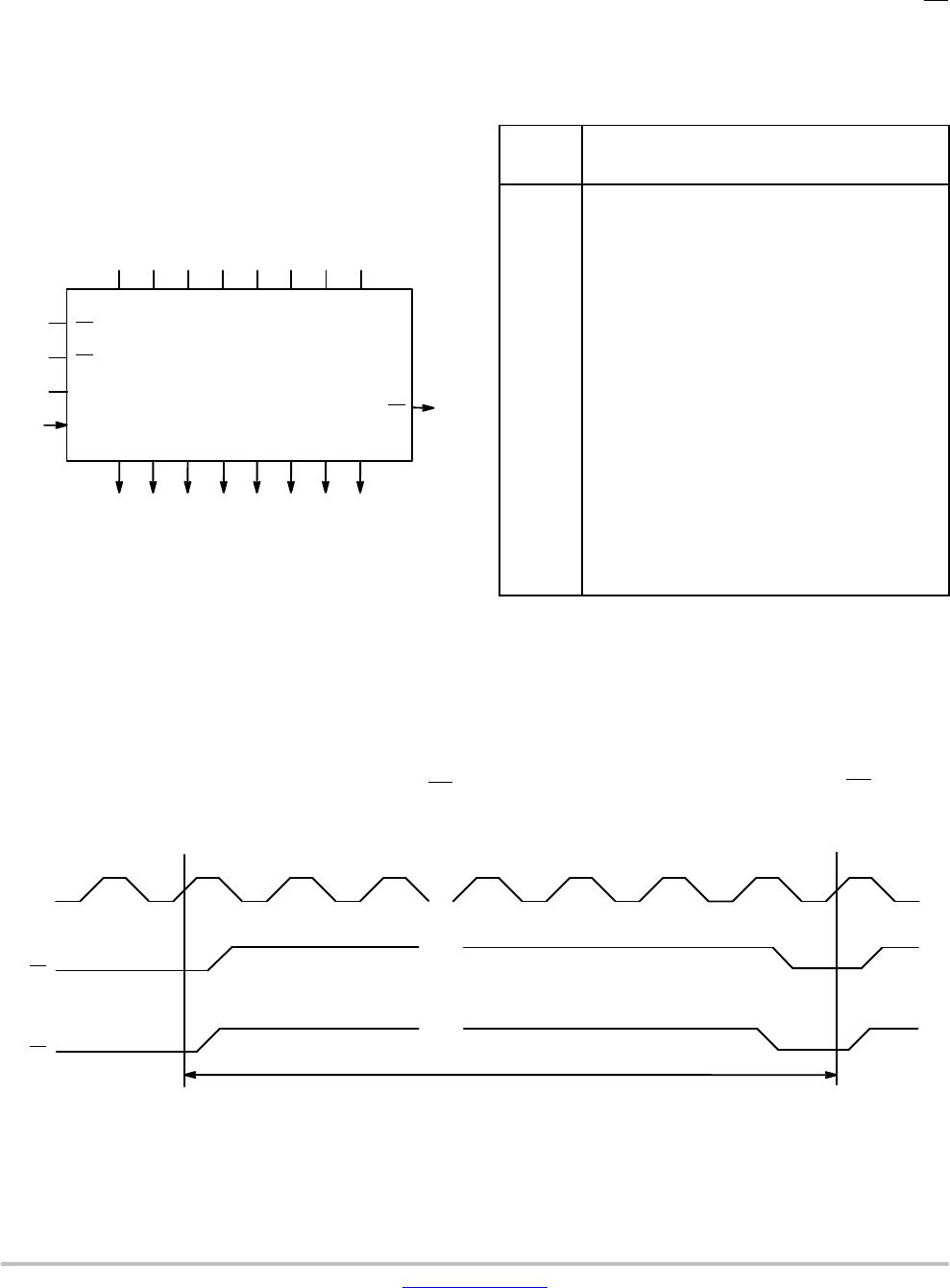
MC10E016, MC100E016
www.onsemi.com
7
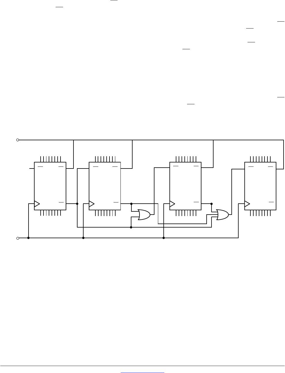
APPLICATIONS INFORMATION
Cascading Multiple E016 Devices
For applications which call for larger than 8-bit counters
multiple E016s can be tied together to achieve very wide bit
width counters. The active low terminal count (TC
) output
and count enable input (CE
) greatly facilitate the cascading
of E016 devices. Two E016s can be cascaded without the
need for external gating, however for counters wider than 16
bits external OR gates are necessary for cascade
implementations.
Figure 3 below pictorially illustrates the cascading of 4
E016s to build a 32-bit high frequency counter. Note the
E101 gates used to OR the terminal count outputs of the
lower order E016s to control the counting operation of the
higher order bits. When the terminal count of the preceding
device (or devices) goes low (the counter reaches an all 1s
state) the more significant E016 is set in its count mode and
will count one binary digit upon the next positive clock
transition. In addition, the preceding devices will also count
one bit thus sending their terminal count outputs back to a
high state disabling the count operation of the more
significant counters and placing them back into hold modes.
Therefore, for an E016 in the chain to count, all of the lower
order terminal count outputs must be in the low state. The bit
width of the counter can be increased or decreased by simply
adding or subtracting E016 devices from Figure 3 and
maintaining the logic pattern illustrated in the same figure.
The maximum frequency of operation for the cascaded
counter chain is set by the propagation delay of the TC
output and the necessary setup time of the CE input and the
propagation delay through the OR gate controlling it (for
16-bit counters the limitation is only the TC
propagation
delay and the CE
setup time). Figure 3 shows EL01 gates
used to control the count enable inputs, however, if the
frequency of operation is lower a slower, ECL OR gate can
be used. Using the worst case guarantees for these
parameters from the ECLinPS data book, the maximum
count frequency for a greater than 16-bit counter is 500 MHz
and that for a 16-bit counter is 625 MHz.
Note that this assumes the trace delay between the TC
outputs and the CE inputs are negligible. If this is not the
case estimates of these delays need to be added to the
calculations.
Figure 3. 32-Bit Cascaded E016 Counter
EL01
CLOCK
P0 -> P7
TC
CLK
P0 -> P7
TCCLK
EL01
P0 -> P7
TC
CLK
P0 -> P7
MSB
E016
PE
CE
Q0 -> Q7Q0 -> Q7 Q0 -> Q7
E016
PE
CE
Q0 -> Q7
E016
PE
CE
LSB
E016
PE
CE
LO
LOAD
TCCLK