LT5572
10
5572f
input (2V
P-P,DIFF
). This maximum RF output level is limited
by the 0.5V
PEAK
maximum baseband swing possible for a
0.5V
DC
common mode voltage level (assuming no extra
negative supply voltage available).
It is possible to bias the LT5572 to a common mode base-
band voltage level other than 0.5V. Table 1 shows the typical
performance for different common mode voltages.
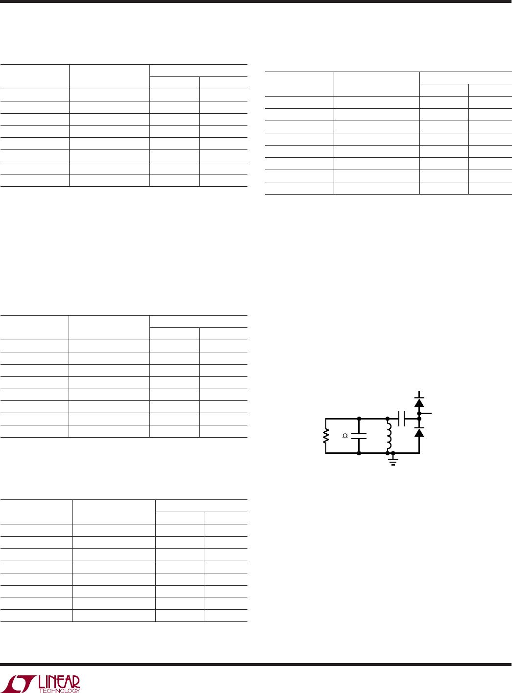
LO section
The internal LO input amplifi er performs single-ended to
differential conversion of the LO input signal. Figure 4
shows the equivalent circuit schematic of the LO input.
The internal, differential LO signal is split into in-phase
and quadrature (90° phase shifted) signals that drive LO
buffer sections. These buffers drive the double balanced I
and Q mixers. The phase relationship between the LO input
and the internal in-phase LO and quadrature LO signals
is fi xed, and is independent of start-up conditions. The
phase shifters are designed to deliver accurate quadrature
signals for an LO frequency near 2GHz. For frequencies
signifi cantly below 1.8GHz or above 2.4GHz, the quadra-
ture accuracy will diminish, causing the image rejection
to degrade. The LO pin input impedance is about 50Ω and
the recommended LO input power is 0dBm. For lower LO
input power, the gain, OIP2, OIP3 and dynamic range will
degrade, especially below –5dBm and at T
A
= 85°C. For
high LO input power (e.g., 5dBm), the LO feedthrough
will increase, without improvement in linearity or gain.
Harmonics present on the LO signal can degrade the
image rejection, because they introduce a small excess
phase shift in the internal phase splitter. For the second (at
4GHz) and third harmonics (at 6GHz) at –20dBc level, the
introduced signal at the image frequency is about –57dBc
or lower, corresponding to an excess phase shift much
less than 1 degree. For the second and third harmonics at
–10dBc, still the introduced signal at the image frequency
is about –47dBc. Higher harmonics than the third will have
less impact. The LO return loss typically will be better than
14dB over the 1.7GHz to 2.4GHz range. Table 2 shows the
LO port input impedance vs frequency.
Table 2. LO Port Input Impedance vs Frequency for EN = High
and P
LO
= 0dBm
FREQUENCY INPUT IMPEDANCE
S
11
(MHz) (Ω)
Mag Angle
1000 45.9+j15.7 0.167 95
1400 60.8+j2.1 0.099 9.4
1600 63.2-j6.0 0.128 –22
1800 61.8-j14.2 0.163 –44
2000 56.4-j16.8 0.165 –61
2200 51.7-j14.7 0.144 –75
2400 47.3-j11.3 0.119 –97
2600 42.5-j8.6 0.122 –126
The input impedance of the LO port is different if the part
is in shutdown mode. The LO input impedance for EN =
Low is given in Table 3.
Table 1. Typical Performance Characteristics vs V
CM
for f
LO
= 2GHz, P
LO
= 0dBm
V
CM
(V) I
CC
(mA) G
V
(dB) OP1dB (dBm) OIP2 (dBm) OIP3 (dBm) NFloor (dBm/Hz) LOFT (dBm) IR (dBc)
0.1 77 –1.3 0.0 47 8.3 –163.2 –45.6 –42.2
0.2 89 –2.7 4.7 45 11.4 –162.2 –42.6 –36.2
0.3 101 –2.1 7.1 49 15.0 –160.9 –42.0 –37.0
0.4 113 –2.0 8.6 51 18.2 –160.2 –42.4 –39.3
0.5 126 –1.9 9.3 52 21.2 –159.2 –42.4 –41.5
0.6 138 –1.9 9.1 52 21.1 –158.6 –42.1 –44.4
APPLICATIO S I FOR ATIO
WUU
U
V
CC
20pF
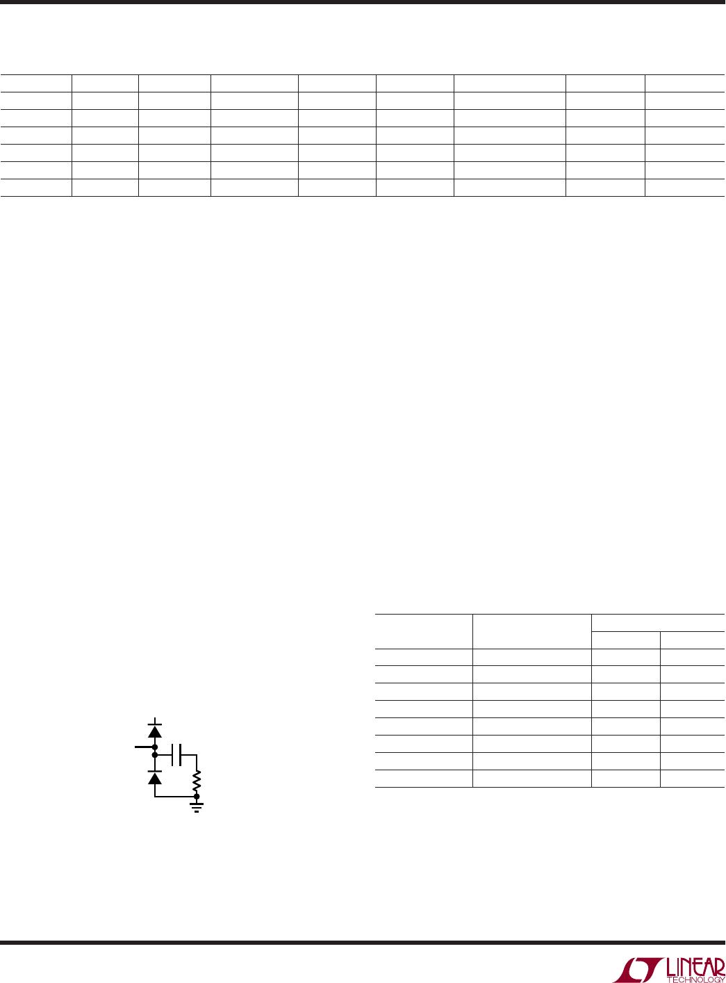
LO
INPUT
Z
IN
≈ 56Ω
5572 F04
Figure 4. Equivalent Circuit Schematic of the LO Input