LT5572
13
5572f
APPLICATIO S I FOR ATIO
WUU
U
Application Measurements
The LT5572 is recommended for basestation applications
using various modulation formats. Figure 10 shows a typical
application. Figure 11 shows the ACPR performance for
W-CDMA using 1-, 2- or 4-channel modulation. Figures
12, 13 and 14 illustrate the 1-, 2- and 4-channel W-CDMA
VCO/SYNTHESIZER
EN
2, 4, 6, 9, 10, 12, 15, 17
I-CH
Q-CH
BALUN
V
CC
V-I
BASEBAND
GENERATOR
V-I
LT5572
5V
14
16
1
7
5
8, 13
5572 TA01a
11
PA
RF = 1.5GHz
TO 2.5GHz
3
I-DAC
Q-DAC
90°
0°
100nF
×2
Figure 10. 1.5GHz to 2.4GHz Direct Conversion Transmitter Application Figure 11. W-CDMA ACPR, ALTCPR and Noise vs RF
Output Power at 2140MHz for 1, 2 and 4 Channels
Figure 12. 1-Channel W-CDMA Spectrum Figure 13. 2-Channel W-CDMA Spectrum Figure 14. 4-Channel W-CDMA Spectrum
RF OUTPUT POWER PER CARRIER (dBm)
–30
ACPR, AltCPR (dBc)
NOISE FLOOR AT 30MHz OFFSET (dBm/Hz)
–70
–60
–10
5572 TA01b
–80
–90
–25
–20
–15
–5
–50
–145
–135
–155
–165
–125
DOWNLINK TEST
MODEL 64 DPCH
4-CH ACPR
2-CH ACPR
1-CH
ACPR
4-CH AltCPR
2-CH AltCPR
1-CH AltCPR
2-CH NOISE
4-CH NOISE
1-CH NOISE
RF FREQUENCY (GHz)
2.1275
–120
POWER IN 30kHz BW (dBm)
–110
–90
–80
–70
2.1375
2.1475
2.1525
–30
5572 F12
–100
2.1325 2.1425
–60
–50
–40
CORRECTED
SPECTRUM
DOWNLINK TEST
MODEL 64 DPCH
UNCORRECTED
SPECTRUM
SPECTRUM
ANALYSER
NOISE FLOOR
RF FREQUENCY (GHz)
2.125
–120
POWER IN 30kHz BW (dBm)
–110
–90
–80
–70
2.145
–30
5572 F13
–100
2.135
2.13
2.15
2.14 2.155
–60
–50
–40
CORRECTED
SPECTRUM
DOWNLINK
TEST MODEL
64 DPCH
UNCORRECTED SPECTRUM
SPECTRUM
ANALYSER
NOISE
FLOOR
RF FREQUENCY (GHz)
2.115
–120
POWER IN 30kHz BW (dBm)
–110
–90
–80
–70
2.135
2.155
2.165
–30
5572 F14
–100
2.125 2.145
–60
–50
–40
CORRECTED
SPECTRUM
DOWNLINK TEST
MODEL 64
DPCH
UNCORRECTED SPECTRUM
SPECTRUM
ANALYSER
NOISE
FLOOR
measurement. To calculate ACPR, a correction is made for
the spectrum analyzer noise fl oor (Application Note 99).
If the output power is high, the ACPR will be limited by the
linearity performance of the part. If the output power is
low, the ACPR will be limited by the noise performance of
the part. In the middle, an optimum ACPR is obtained.
LT5572
14
5572f
APPLICATIO S I FOR ATIO
WUU
U
Figure 15. LO Feedthrough and Image Rejection
vs Temperature After Calibration at 25°C
Figure 16. RF Output Power, Image Rejection and
LO Feedthrough vs Baseband Drive Voltage After
Calibration at 25°C
TEMPERATURE (°C)
–40
–90
LO FEEDTHROUGH (dBm), IR (dB)
–80
–70
–60
–50
–40
–20
02040
5572 F15
60 80
V
CC
= 5V
f
BBI
= 2MHz, 0°
f
BBQ
= 2MHz, 90°
f
LO
= 2GHz
f
RF
= f
BB
+ f
LO
EN = HIGH
P
LO
= 0dB
IMAGE
REJECTION
LO FEEDTHROUGH
CALIBRATED WITH
P
RF
= –10dBm
I AND Q BASEBAND VOLTAGE (V
P-P(DIFF)
)
0
–80
PRF, LOFT (dBm), IR (dBc)
–70
–50
–40
–30
2
4
5
10
P
RF
LO FT
IR
5572 F16
–60
13
–20
–10
0
25°C
85°C
–40°C
V
CC
= 5V
f
BBI
= 2MHz, 0°
f
BBQ
= 2MHz, 90°
EN = HIGH
f
LO
= 2GHz
f
RF
= f
BB
+ f
LO
EN = HIGH
P
LO
= 0dB
Because of the LT5572’s very high dynamic range,
the test equipment can limit the accuracy of the ACPR
measurement. Consult the factory for advice on the ACPR
measurement if needed.
The ACPR performance is sensitive to the amplitude match
of the BBIP and BBIM (or BBQP and BBQM) input voltage.
This is because a difference in AC voltage amplitude will
give rise to a difference in amplitude between the even-order
harmonic products generated in the internal V-I converter.
As a result, they will not cancel out entirely. Therefore, it
is important to keep the amplitudes at the BBIP and BBIM
(or BBQP and BBQM) inputs as equal as possible.
When the temperature is changed after calibration, the
LO feedthrough and the image rejection performance will
change. This is illustrated in Figure 15. The LO feedthrough
and image rejection can also change as a function of the
baseband drive level as depicted in Figure 16.
LT5572
15
5572f
PACKAGE DESCRIPTIO
U
Information furnished by Linear Technology Corporation is believed to be accurate and reliable.
However, no responsibility is assumed for its use. Linear Technology Corporation makes no represen-
tation that the interconnection of its circuits as described herein will not infringe on existing patent rights.
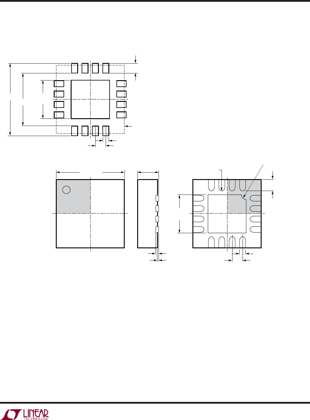
UF Package
16-Lead Plastic QFN (4mm × 4mm)
(Reference LTC DWG # 05-08-1692)
4.00 ± 0.10
(4 SIDES)
NOTE:
1. DRAWING CONFORMS TO JEDEC PACKAGE OUTLINE MO-220 VARIATION (WGGC)
2. DRAWING NOT TO SCALE
3. ALL DIMENSIONS ARE IN MILLIMETERS
4. DIMENSIONS OF EXPOSED PAD ON BOTTOM OF PACKAGE DO NOT INCLUDE
MOLD FLASH. MOLD FLASH, IF PRESENT, SHALL NOT EXCEED 0.15mm ON ANY SIDE
5. EXPOSED PAD SHALL BE SOLDER PLATED
6. SHADED AREA IS ONLY A REFERENCE FOR PIN 1 LOCATION
ON THE TOP AND BOTTOM OF PACKAGE
PIN 1
TOP MARK
(NOTE 6)
0.55 ± 0.20
1615
1
2
BOTTOM VIEW—EXPOSED PAD
2.15 ± 0.10
(4-SIDES)
0.75 ± 0.05
R = 0.115
TYP
0.30 ± 0.05
0.65 BSC
0.200 REF
0.00 – 0.05
(UF16) QFN 10-04
RECOMMENDED SOLDER PAD PITCH AND DIMENSIONS
0.72 ±0.05
0.30 ±0.05
0.65 BSC
2.15 ± 0.05
(4 SIDES)
2.90 ± 0.05
4.35 ± 0.05
PACKAGE OUTLINE
PIN 1 NOTCH R = 0.20 TYP
OR 0.35 × 45° CHAMFER

LT5572EUF#PBF

Mfr. #:
Manufacturer:
Analog Devices Inc.
Description:
Modulator / Demodulator 2GHz Direct Quadrature Modulator w/ HiZ & 0.5V Bias
Lifecycle:
New from this manufacturer.
Delivery:
DHL FedEx Ups TNT EMS
Payment:
T/T Paypal Visa MoneyGram Western Union

Products related to this Datasheet