3
INDUSTRIAL TEMPERATURE RANGE
IDT5V2305
2.5V TO 3.3V HIGH PERFORMANCE CLOCK BUFFER
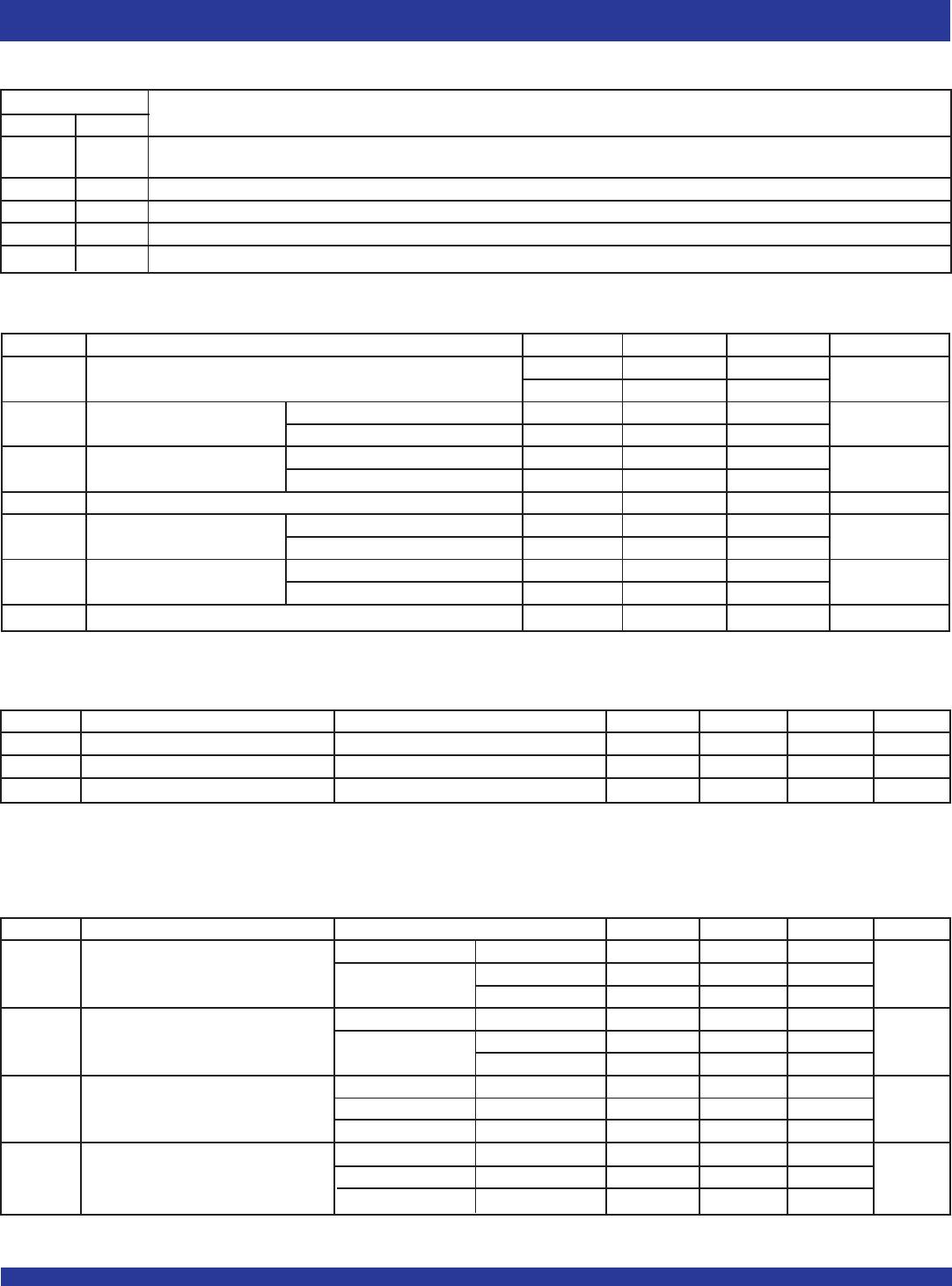
Symbol Description Min. Typ. Max. Unit
V
DD Internal Power Supply Voltage 2.3 2.5 V
3.3 3.6
V
IL Input Voltage LOW VDD = 3V to 3.6V 0.8 V
VDD = 2.3V to 2.7V 0.7
VIH Input Voltage HIGH VDD = 3V to 3.6V 2 V
VDD = 2.3V to 2.7V 1.7
VI Input Voltage 0 VDD V
IOH Output Current HIGH VDD = 3V to 3.6V -12 mA
VDD = 2.3V to 2.7V -6
I
OL Output Current LOW VDD = 3V to 3.6V 12 mA
VDD = 2.3V to 2.7V 6
T
A Ambient Operating Temperature -40 +85 °C
RECOMMENDED OPERATING RANGE
NOTE:
1. All typical values are at respective nominal VDD.
DC ELECTRICAL CHARACTERISTICS - VDD = 3.3V ± 0.3V
Symbol Parameter Test Conditions Min. Typ.
(1)
Max Unit
V
DD = Min. to Max. IOH = -100μAVDD - 0.2
VOH HIGH level Output Voltage VDD = 3V IOH = -12mA 2.1 V
IOH = -6mA 2.4
V
DD = Min. to Max. IOH = 100μA 0.2
VOL LOW level Output Voltage VDD = 3V IOH = 12mA 0.8 V
IOH = 6mA 0.55
V
DD = 3V VO = 1V -28
IOH HIGH level Output Current VDD = 3.3V VO = 1.65V -36 mA
VDD = 3.6V VO = 3.135V -14
V
DD = 3V VO = 1.95V 28
IOL LOW level Output Current VDD = 3.3V VO = 1.65V 36 mA
V
DD = 3.6V VO = 0.4V 14
NOTE:
1. For IDD over frequency, see TEST CIRCUIT AND WAVEFORMS.
DC ELECTRICAL CHARACTERISTICS OVER OPERATING RANGE
Symbol Parameter Test Conditions Min. Typ. Max Unit
VIK Input Voltage VDD = 3V, IIN = -18mA - 1.2 V
IIN Input Current VI = 0V or VDD ±5 μA
I
DD Static Device Current
(1)
CLK = 0V or VDD, IO = 0mA, VDD = 3.3V 25 μA
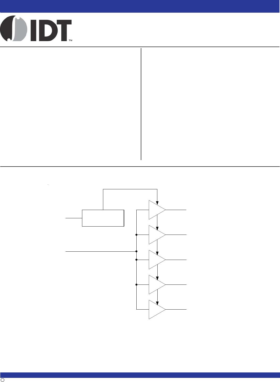
PIN DESCRIPTION
TERMINAL
Symbol I/O Description
G I Output Enable Control for Y(0:4) Outputs. This output enable is active HIGH. If this pin is Logic HIGH, the Y(0:4) clock outputs will follow the
input clock (CLK). If this pin is logic LOW, the Y(0:4) outputs will drive low independent of the state of CLK.
Y(0:4) O Buffered Output Clocks
CLK I Input Reference Frequency
GND Ground
V
DD PWR DC Power Supply, 2.3V to 3.6V