5
INDUSTRIAL TEMPERATURE RANGE
IDT5V2305
2.5V TO 3.3V HIGH PERFORMANCE CLOCK BUFFER
SWITCHING CHARACTERISTICS OVER OPERATING RANGE -
V
DD = 2.5V ± 0.2V
(1)
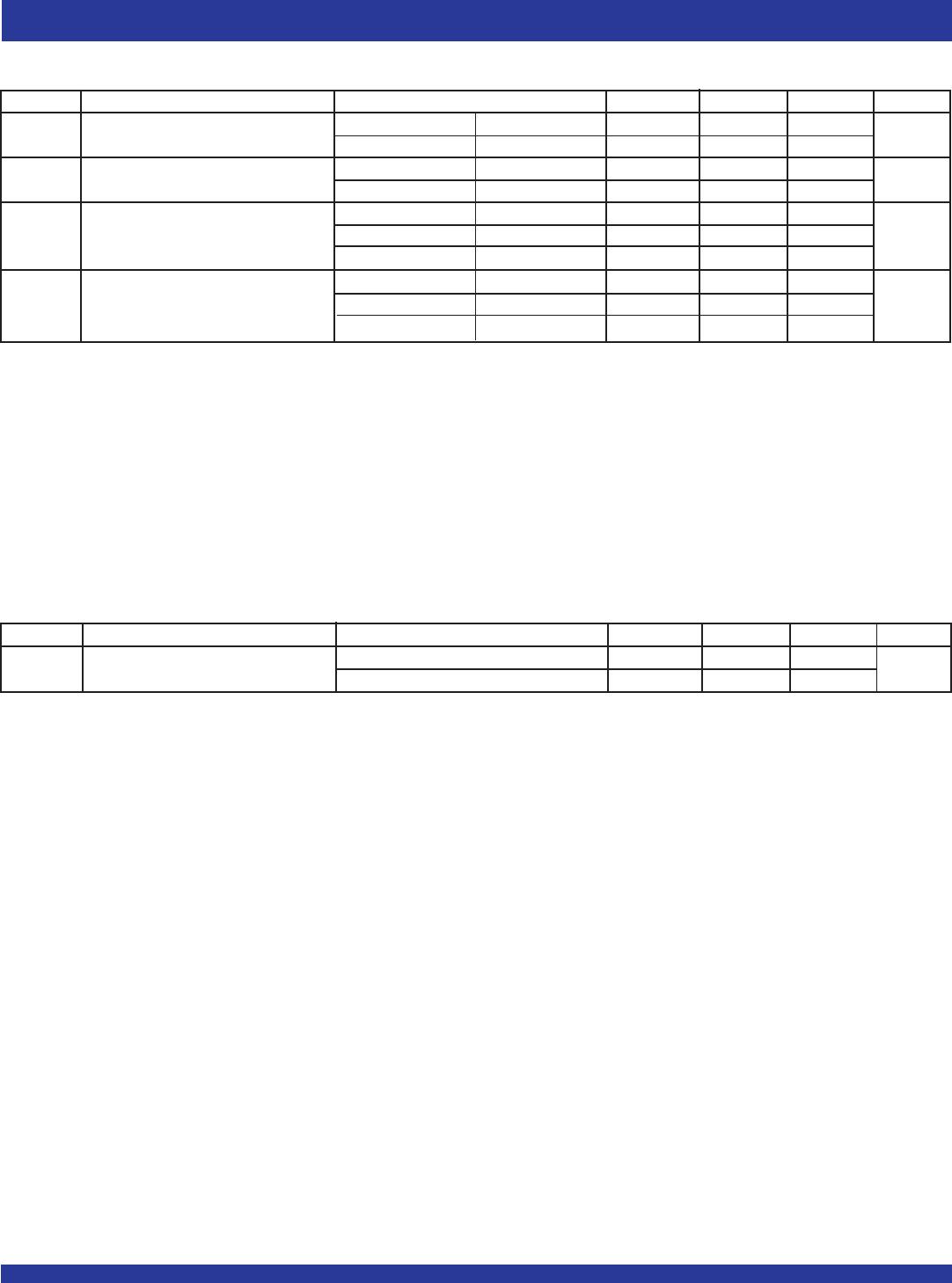
Symbol Parameter Test Conditions Min. Typ.
(1)
Max Unit
t
PLH CLK to Yx f = 0MHz to 170MHz, CL = 25pF 1.5 3 ns
tPHL
tSK(O)
(2)
Output Skew, Yx to Yx 100 ps
tSK(P) Pulse Skew 350 ps
tSK(PP) Part-to-Part Skew 600 ps
tR Rise Time VO = 0.4V to 1.7V
(3)
0.4 1.625 V/ns
tF Fall Time VO = 1.7V to 0.4V
(3)
0.4 1.625 V/ns
tSU G before CLK↓ V(THRESHOLD) = VDD/2 0.1 ns
t
H G after CLK↓ 0.4
NOTES:
1. All typical values are at respective nominal VDD.
2. This specification is only valid for equal loading of all outputs.
3. Measured at 100MHz.
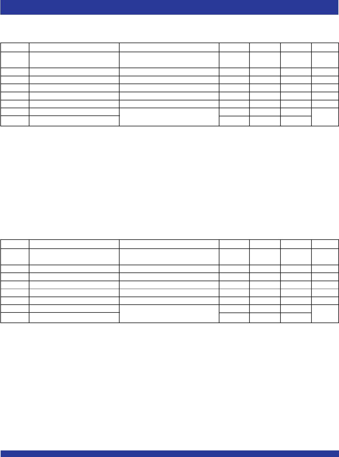
SWITCHING CHARACTERISTICS OVER OPERATING RANGE -
V
DD = 3.3V ± 0.3V
(1)
Symbol Parameter Test Conditions Min. Typ.
(1)
Max Unit
t
PLH CLK to Yx f = 0MHz to 200MHz, CL = 25pF 1.3 2.6 ns
tPHL
tSK(O)
(2)
Output Skew, Yx to Yx 75 ps
tSK(P) Pulse Skew 200 ps
tSK(PP) Part-to-Part Skew 500 ps
tR Rise Time VO = 0.4V to 2V
(3)
1.0 2.3 V/ns
tF Fall Time VO = 2V to 0.4V
(3)
1.0 2.3 V/ns
t
SU G before CLK↓ V(THRESHOLD) = VDD/2 0.1 ns
t
H G after CLK↓ 0.4
NOTES:
1. All typical values are at respective nominal VDD.
2. This specification is only valid for equal loading of all outputs.
3. Measured at 100MHz.