1©2018 Integrated Device Technology, Inc. July 5, 2018
Description
The 9FGV1006 is a member of IDT's PhiClock™ programmable
clock generator family. The 9FGV1006 provides two copies of a
single integer, fractional or spread spectrum output frequency and
one copy of the crystal reference input. Two select pins allow for
hardware selection of the desired configuration, or two I
2
C bits
allow easy software selection of the desired configuration. The
user may configure any one of the four OTP configurations as the
default when operating in I
2
C mode. Four unique I
2
C addresses
are available, allowing easy I
2
C access to multiple components.
Typical Applications
▪ HPC
▪ Storage
▪ 10G/25G Ethernet
▪ Fiber Optic Modules
▪ SSDs
▪ NVLink
Output Features
▪ 1 integer, fractional or spread spectrum output frequency per
configuration
▪ 2 programmable output pairs plus 1 LVCMOS REF output
▪ 10MHz–325MHz output frequency (LVDS or LP-HCSL), integer
configuration
▪ 10MHz–200MHz output frequency (LVCMOS), integer
configuration
▪ 10MHz–156.25MHz output frequency (LVDS or LP-HCSL),
fractional or spread spectrum configuration
Features
▪ 1.8V to 3.3V V
DD
s and V
DDREF
▪ Individual 1.8V to 3.3V V
DDO
for each output pair
▪ Supports HCSL, LVDS and LVCMOS I/O standards
▪ Supports LVPECL and CML logic with easy AC coupling – see
application note AN-891
for alternate terminations
▪ HCSL utilizes IDT's LP-HCSL technology for improved
performance, lower power and higher integration:
• Programmable output impedance of 85 or 100Ω
▪ On-board OTP supports up to 4 complete configurations
▪ Configuration selected via strapping pins or I
2
C
▪ < 100mW at 1.8V, < 200mW at 3.3V with outputs running at
100MHz
▪ 4 programmable I
2
C addresses: D0/D1, D2/D3, D4/D5, D6/D7
read/write
▪ Supported by IDT Timing Commander™ software
▪ 3 × 3 mm 16-LGA with integrated crystal option (9FGV1006Q)
Key Specifications
▪ 298fs rms typical phase jitter outputs at 156.25MHz (12kHz–
20MHz)
▪ PCIe Gen1– 4 compliant
PCIe Clocking Architectures
▪ Common Clocked (CC)
▪ Independent Reference without spread spectrum (SRnS)
▪ Independent Reference with spread spectrum (SRIS)
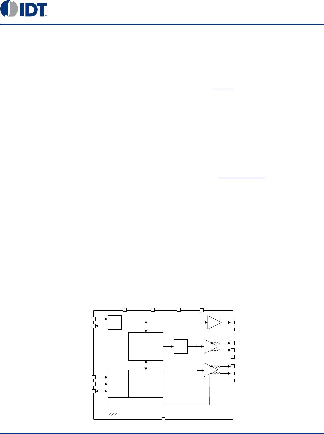
Block Diagram
^SEL1/SDA
Fractional
PLL
(SSC)
VDDREFp
XO
XIN/CLKIN
VDDDp VDDAp
^SEL0/SCL
OUT0
OUT0#
vSEL_I2C#
EPAD/GND
REF0
Internal terminations are available when LP-HCSL output format is selected.
OSC
OTP_VPP
INT
DIV
OUT1#
OUT1
VDDO1
VDDO0
VDDAO0p
Factory
Configuration
SMBus
Engine
Control Logic
9FGV1006
Datasheet
Low Phase-Noise, Low-Power
Programmable PhiClock™ Generator