2
LTC2847
sn2847 2847fs
ORDER PART
NUMBER
(Note 1)
V
CC
Voltage.............................................. –0.3V to 6.5V
V
IN
Voltage .............................................. –0.3V to 6.5V
Input Voltage
Transmitters ........................... –0.3V to (V
CC
+ 0.3V)
Receivers............................................... –18V to 18V
Logic Pins .............................. –0.3V to (V
CC
+ 0.3V)
Output Voltage
Transmitters ................. (V
EE
– 0.3V) to (V
DD
+ 0.3V)
Receivers................................. –0.3V to (V
IN
+ 0.3V)
V
EE
........................................................ –10V to 0.3V
V
DD
....................................................... –0.3V to 10V
Short-Circuit Duration
Transmitter Output ..................................... Indefinite
Receiver Output.......................................... Indefinite
V
EE
.................................................................. 30 sec
Operating Temperature Range
LTC2847C ............................................... 0°C to 70°C
LTC2847I........................................... –40°C to 85°C
Storage Temperature Range ................ –65°C to 150°C
Lead Temperature (Soldering, 10 sec)................. 300°C
LTC2847CUHF
LTC2847IUHF
ABSOLUTE AXI U RATI GS
WWWU
PACKAGE/ORDER I FOR ATIO
UU
W
The ● denotes specifications which apply over the full operating
temperature range, otherwise specifications are at T
A
= 25°C. V
CC
= 5V, V
IN
= 3.3V, unless otherwise noted (Notes 2, 3)
ELECTRICAL CHARACTERISTICS
Consult LTC Marketing for parts specified with wider operating temperature ranges.
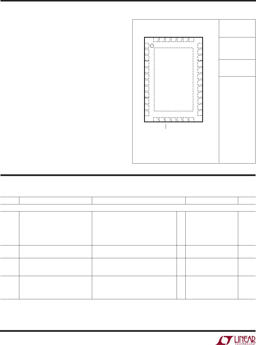
UHF PART
MARKING
2847
2847I
13 14 15 16
TOP VIEW
UHF PACKAGE
38-LEAD (7mm × 5mm) PLASTIC QFN
UNDERSIDE METAL INTERNALLY CONNECTED TO V
EE
(PCB CONNECTION OPTIONAL)
17 18 19
38 37 36 35 34 33 32
24
25
26
27
28
29
30
31
8
7
6
5
4
3
2
1
23
22
21
20
9
10
11
12
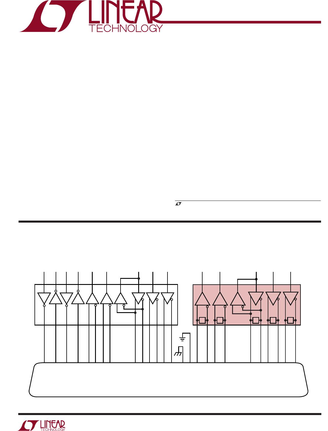
NC
V
DD
NC
V
CC
D1
D2
D3
R1
R2
R3
M0
M1
V
IN
M2
DCE/DTE
R3 B
R3 A
NC
NC
C1
+
C1
–
V
EE
C2
+
C2
–
V
EE
V
EE
GND
GND
D1 A
D1 B
D2 A
D2 B
D3/R1 A
D3/R1 B
NC
NC
R2 A
R2 B
T
JMAX
= 125°C, θ
JA
= 34°C/W
SYMBOL PARAMETER CONDITIONS MIN TYP MAX UNITS
Supplies
I
CC
V
CC
Supply Current (DCE Mode, RS530, RS530-A, X.21 Modes, No Load 14 mA
All Digital Pins = GND or V
IN
) RS530, RS530-A, X.21 Modes, Full Load ● 100 130 mA
V.35 Mode
● 126 170 mA
V.28 Mode, No Load 20 mA
V.28 Mode, Full Load
● 35 75 mA
No-Cable Mode
● 300 900 µA
I
VIN
V
IN
Supply Current All Modes Except No-Cable Mode 405 µA
(DCE Mode, All Digital Pins = GND or V
IN
)
P
D
Internal Power Dissipation (DCE Mode) RS530, RS530-A, X.21 Modes, Full Load 410 mW
V.35 Mode, Full Load 625 mW
V.28 Mode, Full Load 150 mW
V
+
Positive Charge Pump Output Voltage V.11 or V.28 Mode, No Load ● 8 9.3 V
V.35 Mode
● 7 8.0 V
V.28 Mode, with Load
● 8 8.7 V
V.28 Mode, with Load, I
DD
= 10mA 6.5 V