© Semiconductor Components Industries, LLC, 2016
April, 2016 − Rev. 7
1 Publication Order Number:
ESD5481/D
ESD5481
ESD Protection Diodes
Micro−Packaged Diodes for ESD Protection
The ESD5481 is designed to protect voltage sensitive components
from ESD. Excellent clamping capability, low leakage, and fast
response time provide best in class protection on designs that are
exposed to ESD. Because of its small size, it is suited for use in cellular
phones, MP3 players, digital cameras and many other portable
applications where board space comes at a premium.
Specification Features
• Low Capacitance 15 pF
• Low Clamping Voltage
• Small Body Outline Dimensions: 0.60 mm x 0.30 mm
• Low Body Height: 0.3 mm
• Stand−off Voltage: 5.0 V
• Low Leakage
• Response Time is < 1 ns
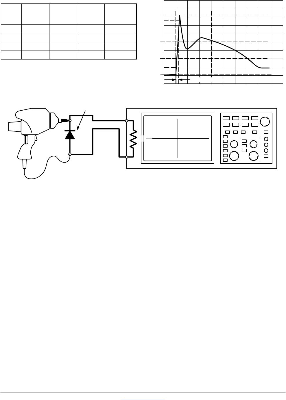
• IEC61000−4−2 Level 4 ESD Protection
• IEC61000−4−4 Level 4 EFT Protection
• These Devices are Pb−Free, Halogen Free/BFR Free and are RoHS
Compliant
Mechanical Characteristics
MOUNTING POSITION:
Any
QUALIFIED MAX REFLOW TEMPERATURE: 260°C
Device Meets MSL 1 Requirements
MAXIMUM RATINGS
Rating Symbol Value Unit
IEC 61000−4−2 (ESD) Contact
Air
±20
±20
kV
IEC 61000−4−4 (EFT) 5/50 ns 40 A
Total Power Dissipation on FR−5 Board
(Note 1) @ T
A
= 25°C
Thermal Resistance, Junction−to−Ambient
°P
D
°
R
q
JA
300
400
mW
°C/W
Junction and Storage Temperature Range T
J
, T
stg
−55 to +150 °C
Lead Solder Temperature − Maximum
(10 Second Duration)
T
L
260 °C
Stresses exceeding those listed in the Maximum Ratings table may damage the
device. If any of these limits are exceeded, device functionality should not be
assumed, damage may occur and reliability may be affected.
1. FR−5 = 1.0 x 0.75 x 0.62 in.
See Application Note AND8308/D for further description of survivability specs.
Device Package Shipping
†
ORDERING INFORMATION
†For information on tape and reel specifications,
including part orientation and tape sizes, please
refer to our Tape and Reel Packaging Specification
Brochure, BRD8011/D.
www.onsemi.com
ESD5481MUT5G X3DFN2
(Pb−Free)
10,000 /
Tape & Reel
X3DFN2
CASE 152AF
MARKING
DIAGRAM
12
PIN 1
A = Specific Device Code
M = Date Code
A M