INDUSTRIAL TEMPERATURE RANGE
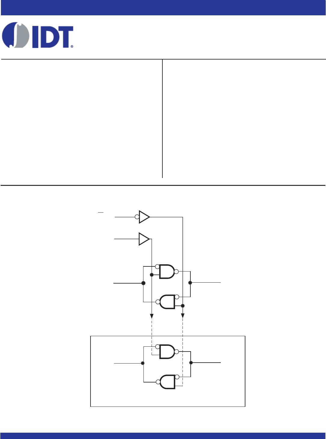
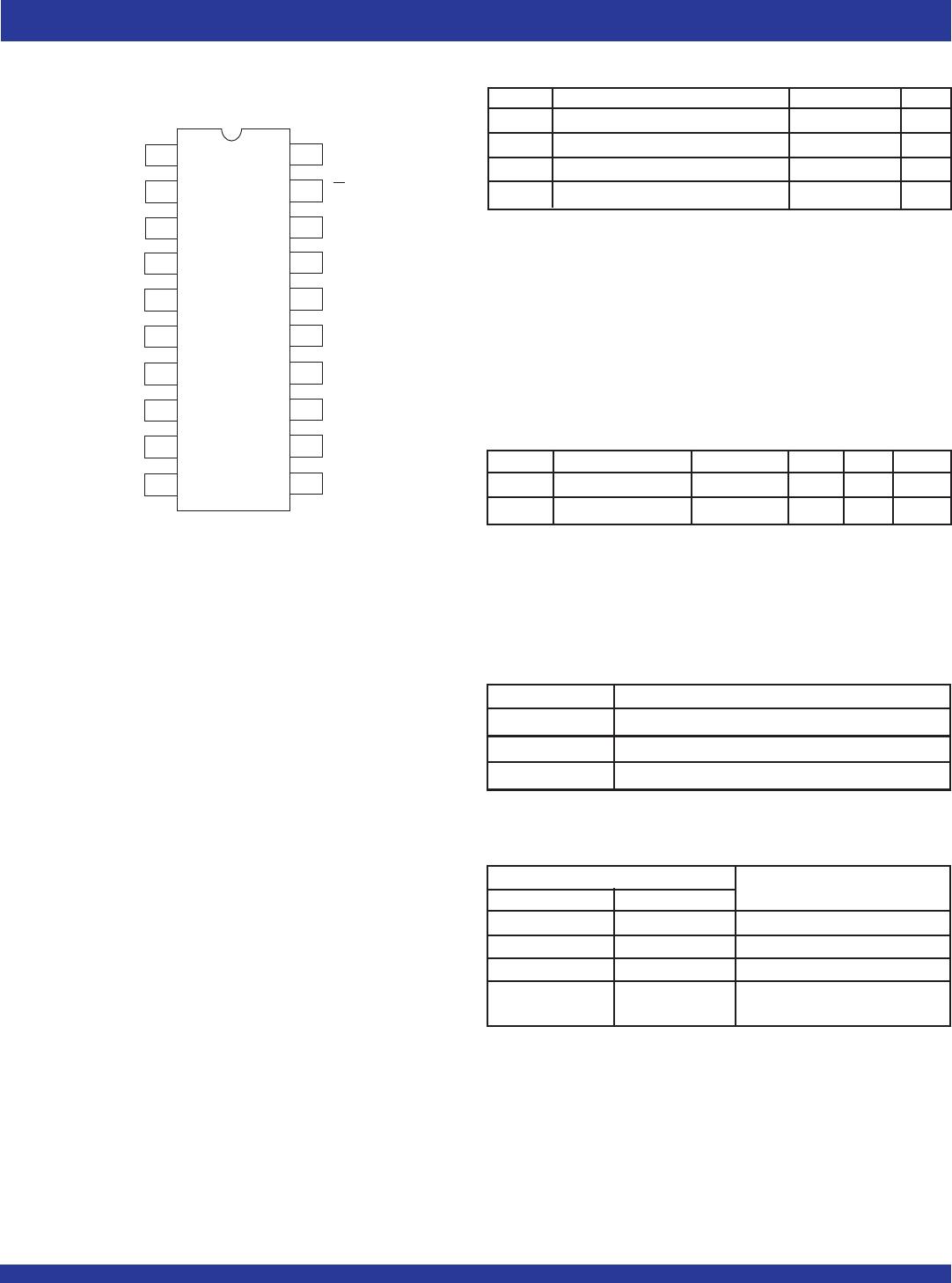
IDT74FCT621T/AT
FAST CMOS OCTAL BUS TRANSCEIVER (OPEN DRAIN)
3
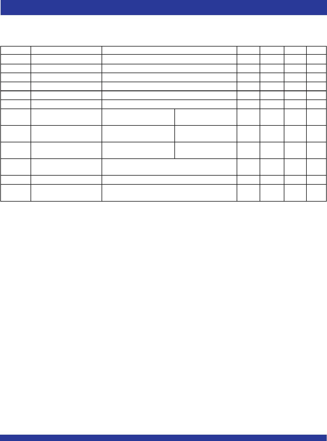
DC ELECTRICAL CHARACTERISTICS OVER OPERATING RANGE
Following Conditions Apply Unless Otherwise Specified:
Industrial: TA = –40°C to +85°C, VCC = 5.0V ±5%
Symbol Parameter Test Conditions
(1)
Min. Typ.
(2)
Max. Unit
VIH Input HIGH Level Guaranteed Logic HIGH Level 2 — — V
VIL Input LOW Level Guaranteed Logic LOW Level — — 0.8 V
IIH Input HIGH Current
(4)
VCC = Max., VI = 2.7V — — ±1 µA
IIL Input LOW Current
(4)
VCC = Max., VI = 0.5V — — ±1 µA
II Input HIGH Current
(4)
VCC = Max., VI = VCC (Max.) — — ±1 µA
VIK Clamp Diode Voltage VCC = Min., IN= –18mA — –0.7 –1.2 V
I
OH Output HIGH Current VCC = Max. VOH = Vcc (Max.) — — 20 µA
VIN = VIH or VIL
VOL Output LOW Voltage VCC = Min. IOL = 64mA
(3)
— 0.3 0.55 V
(B Bus) VIN = VIH or VIL
VOL Output LOW Voltage VCC = Min. IOL = 48mA
(3)
— 0.3 0.5 V
(A Bus) VIN = VIH or VIL
IOFF Input/Output Power Off VCC = 0V, VIN or VO - 4.5V — — ±1 µA
Leakage
(4)
VH Input Hysteresis — — 200 — mV
I
CC Quiescent Power Supply VCC = max., VIN = GND or Vcc — 0.01 1 mA
Current
NOTES:
1. For conditions shown as Max. or Min., use appropriate value specified under Electrical Characteristics for the applicable device type.
2. Typical values are at VCC = 5.0V, +25°C ambient.
3. These are maximum IOL values per output, for 8 outputs turned on simultaneously. Total maximum IOL (all outputs) is 512mA for commercial and 384mA for military. Derate
IOL for number of outputs exceeding 8 turned on simultaneously.
4. The test limit for this parameter is ±5µA at TA = –55°C.