INDUSTRIAL TEMPERATURE RANGE
4
IDT74FCT621T/AT
FAST CMOS OCTAL BUS TRANSCEIVER (OPEN DRAIN)
NOTES:
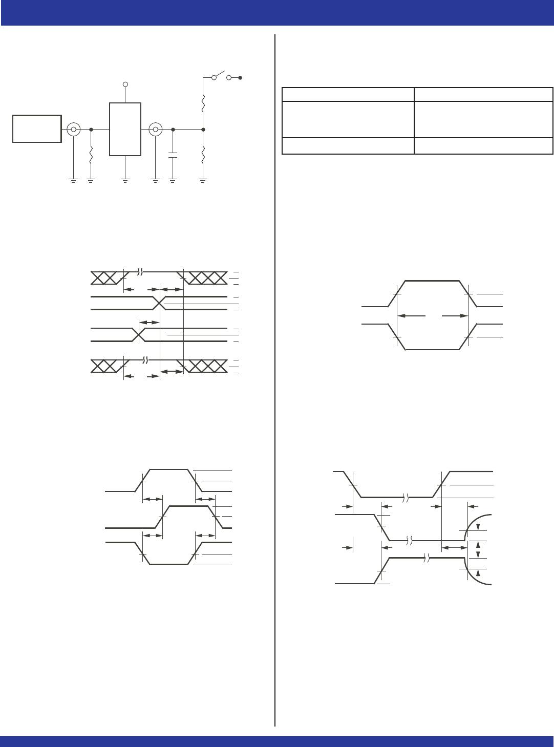
1. See test circuit and waveforms.
2. Minimum limits are guaranteed but not tested on Propagation Delays.
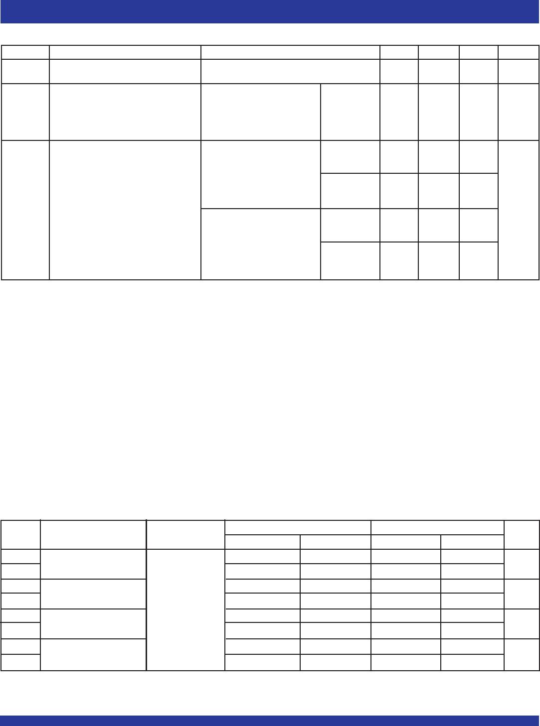
IDT74FCT621T IDT74FCT621AT
Symbol Parameter Condition
(1)
Min.
(2)
Max. Min.
(2)
Max. Unit
tPLH Propagation Delay, A to B CL = 50pF 5.5 13 5.5 12 ns
tPHL RL = 500Ω 1.5 8.5 1.5 6.8
tPLH Propagation Delay, B to A 5.5 12.5 5.5 12 ns
tPHL 1.5 8 1.5 6.4
tPLH Propagation Delay, GBA to A 5.5 14 5.5 13 ns
tPHL 1.5 8.5 1.5 6.8
t
PLH Propagation Delay, GAB to B 5.5 14 5.5 13 ns
tPHL 1.5 8 1.5 6.4
SWITCHING CHARACTERISTICS OVER OPERATING RANGE
POWER SUPPLY CHARACTERISTICS
Symbol Parameter Test Conditions
(1)
Min. Typ.
(2)
Max. Unit
ΔI
CC Quiescent Power Supply Current VCC = Max. — 0.5 2 mA
TTL Inputs HIGH V
IN = 3.4V
(3)
ICCD Dynamic Power Supply Current
(4)
Vcc = Max. VIN = VCC — 0.15 0.25 mA/MHz
Outputs Open VIN = GND
GBA = GAB = GND or VCC
One Input Toggling
50% Duty Cycle
I
C Total Power Supply Current
(6,7)
Vcc = Max. VIN = VCC — 1.5 3.5 mA
Outputs Open V
IN = GND
GBA = GAB = GND or VCC
One Bit Toggling VIN = 3.4V — 1.8 4.5
at fi =10MHz VIN = GND
50% Duty Cycle
Vcc = Max. VIN = VCC —36
(5)
Outputs Open VIN = GND
GBA = GAB = GND or V
CC
Eight Bits Toggling VIN = 3.4V — 5 14
(5)
at fi = 2.5MHz VIN = GND
50% Duty Cycle
NOTES:
1. For conditions shown as Max. or Min., use appropriate value specified under Electrical Characteristics for the applicable device type.
2. Typical values are at VCC = 5.0V, +25°C ambient.
3. Per TTL driven input (VIN = 3.4V); all other inputs at VCC or GND.
4. This parameter is not directly testable, but is derived for use in Total Power Supply Calculations.
5. Values for these conditions are examples of the ICC formula. These limits are guaranteed but not tested.
6. IC = IQUIESCENT + IINPUTS + IDYNAMIC
IC = ICC + ΔICC DHNT + ICCD (fCP/2 + fiNi)
ICC = Quiescent Current
ΔICC = Power Supply Current for a TTL High Input (VIN = 3.4V)
DH = Duty Cycle for TTL Inputs High
NT = Number of TTL Inputs at DH
ICCD = Dynamic Current Caused by an Output Transition Pair (HLH or LHL)
fCP = Clock Frequency for Register Devices (Zero for Non-Register Devices)
fi = Input Frequency
Ni = Number of Inputs at fi
All currents are in milliamps and all frequencies are in megahertz.
7. This test is performed with outputs tied to GND through a pull-down resistor.