Enhanced Product HMC470A-EP
Rev. 0 | Page 5 of 8
PIN CONFIGURATION AND FUNCTION DESCRIPTIONS
12
11
10
1
3
4
9
2
6
5
7
8
16
15
14
13
VDD
RF1
NIC
ACG1
V1
V2
V3
V4
V5
RF2
NIC
ACG6
ACG2
ACG3
ACG4
ACG5
NOTES
1. NIC = THESE PINS ARE NOT INTERNALLY CONNECTED;
HOWEVER, ALL DATA SHOWN HEREIN WAS
MEASURED WHEN THESE PINS CONNECTED TO RF/DC
GROUND OF EVALUATION BOARD.
2. EXPOSED PAD. THE EXPOSED PAD MUST BE
CONNECTED TO GROUND FOR PROPER OPERATION.
16364-004
HMC470A-EP
TOP VIEW
(Not to Scale)
Figure 4. Pin Configuration
Table 4. Pin Function Descriptions
Pin No. Mnemonic Description
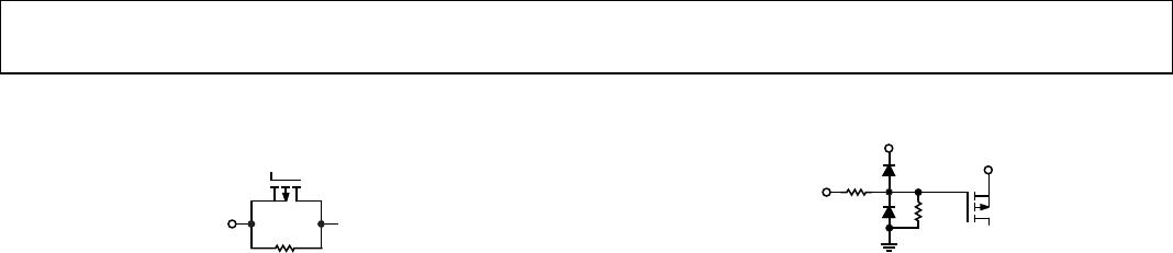
1 VDD Power Supply. See Figure 6 for the interface schematic.
2 RF1
RF Input or Output of the Attenuator. The RF1 pin is dc-coupled to VDD and ac matched to 50 Ω. An external
dc blocking capacitor is required. Select the capacitor value for the lowest frequency of operation. See Figure 5
for the interface schematic.
3, 10 NIC
Not Internally Connected. These pins are not internally connected; however, all data shown herein was
measured when these pins were connected to the RF/dc ground of the evaluation board.
4 to 9 ACG1 to ACG6
AC Grounding Capacitor Pins. Leave these pins not connected when operating above 700 MHz. For
frequencies less than 700 MHz, connect capacitors larger than 100 pF as close to the ACGx pins as possible.
Select the capacitor value for the lowest frequency of operation.
RF Input or Output of the Attenuator. The RF2 pin is dc-coupled to VDD and ac matched to 50 Ω. An external
dc blocking capacitor is required. Select the capacitor value for the lowest frequency of operation. See Figure 5
for the interface schematic.
12 to 16 V1 to V5
Parallel Control Voltage Inputs. These pins select the required attenuation (see Table 5). See Figure 6 for the
interface schematic.
EPAD Exposed Pad. The exposed pad must be connected to ground for proper operation.
Table 5. P4 to P0 Truth Table
Digital Control Input
1
V1 V2 V3 V4 V5 Attenuation State (dB)
High High High High Low 1
High High High Low High 2
High High Low High High 4
High Low High High High 8
Low High High High High 16
1
Any combination of the control voltage input states shown in Table 5 provides an attenuation equal to the sum of the bits selected.