TEA19162T All information provided in this document is subject to legal disclaimers. © NXP Semiconductors N.V. 2016. All rights reserved.
Product data sheet Rev. 1 — 10 March 2016 21 of 30
NXP Semiconductors
TEA19162T
PFC controller
T
p
pulse period x-capacitor discharge;
pulseduration<2ms (typical);
GATEPFC pin
3.76 4.00 4.27 ms
V
dis(dch)GATEPFC
disable discharge
voltage on pin
GATEPFC
x-capacitor discharge 9.00 9.45 9.90 V
V
dis(dch)SNSCUR
disable discharge
voltage on pin
SNSCUR
x-capacitor discharge 44 50 56 mV
Output voltage sensing, regulation and compensation (SNSBOOST and PFCCOMP pins)
V
reg(SNSBOOST)
regulation voltage
on pin SNSBOOST
I
PFCCOMP
= 0 A 2.475 2.500 2.525 V
g
m
transconductance error amplifier; V
SNSBOOST
to I
PFCCOMP
;
|V
SNSBOOST
V
intregd(SNSBOOST)
|<40mV
90 75 60 A/V
I
sink(PFCCOMP)
sink current on pin
PFCCOMP
V
SNSBOOST
=2V; V
PFCCOMP
= 2.75 V 30.0 35.5 41.0 A
g
m(high)
high
transconductance
error amplifier; V
SNSBOOST
to I
PFCCOMP
;
V
start(gm)high
V
SNSBOOST
<V
stop(ovp)
- 1.26 - mA/V
V
gm(high)start
start high
transconductance
voltage
pin SNSBOOST 2.56 2.60 2.63 V
I
clamp(max)
maximum clamp
current
pin PFCCOMP; energy save mode;
PFC off; V
PFCCOMP
=0V
260 220 190 A
I
en(PFC)
PFC enable
current
pin PFCCOMP 15 11.5 8 A
V
clamp(PFCCOMP)
clamp voltage on
pin PFCCOMP
bidirectional clamp; energy save mode;
PFC off
3.40 3.50 3.60 V
upper clamp voltage;
unidirectional clamp; operating mode;
PFC on; I
PFCCOMP
=120A
3.70 3.80 3.90 V
lower clamp voltage;
unidirectional clamp; operating mode;
PFC on; V
SNSBOOST
=2.5V;
I
PFCCOMP
=30A
V
ton(max)PFCCOMP
V
Mains compensation
t
on(PFC)
PFC on-time minimum mains voltage compensation
current; V
PFCCOMP
=2V;
V
SNSBOOST
=2.5V;
I
mvc(SNSMAINS)
=5.25A
20 25 30 s
maximum mains voltage compensation
current; V
PFCCOMP
=2V;
V
SNSBOOST
=2.5V;
I
mvc(SNSMAINS)
=I
mvc(SNSMAINS)max
12 3s
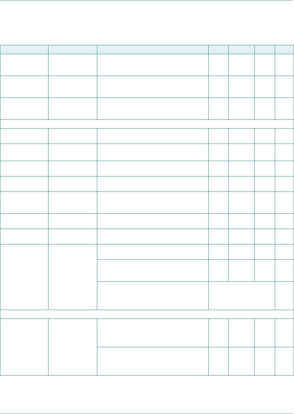
Table 6. Characteristics
…continued
T
amb
=25
C; V
SUPIC
= 20 V; all voltages are measured with respect to ground (pin 2); currents are positive when flowing into
the IC; unless otherwise specified.
Symbol Parameter Conditions Min Typ Max Unit

