XA7A35T-1CSG325Q

DS197 (v1.2) February 23, 2017 www.xilinx.com
Product Specification 1
© Copyright 2014–2017 Xilinx, Inc., Xilinx, the Xilinx logo, Artix, ISE, Kintex, Spartan, UltraScale, Virtex, Vivado, Zynq, and other designated brands included herein are
trademarks of Xilinx in the United States and other countries. PCI, PCIe, and PCI Express are trademarks of PCI-SIG and used under license. All other trademarks are the
property of their respective owners.
General Description
Xilinx® XA Artix®-7 (Automotive) FPGAs are optimized for the lowest cost and power with small form-factor packaging for high-volume automotive
applications. Designers can leverage more logic per watt compared to the Spartan®-6 family.
Built on a state-of-the-art high-performance/low-power (HPL) 28 nm high-k metal gate (HKMG) process technology, XA Artix-7 FPGAs redefine low-cost
alternatives with more logic per watt. Unparalleled increase in system performance with 52 Gb/s I/O bandwidth, 100,000 logic cell capacity, 264 GMAC/s
DSP, and flexible built-in DDR3 memory interfaces enable a new class of high-throughput, low-cost automotive applications. XA Artix-7 FPGAs also offer
many high-end features, such as integrated advanced Analog Mixed Signal (AMS) technology. Analog becomes the next level of integration through the
seamless implementation of independent dual 12-bit, 1 MSPS, 17-channel analog-to-digital converters. Most importantly, XA Artix-7 FPGAs proudly meet
the high standards of the automotive grade with a maximum temperature of 125°C.
Summary of XA Artix-7 FPGA Features
Automotive Temperatures:
I-Grade: Tj= –40°C to +100°C
Q-Grade: Tj= –40°C to +125°C
Automotive Standards:
ISO-TS16949 compliant
AEC-Q100 qualification
Production Part Approval Process (PPAP) documentation
Beyond AEC-Q100 qualification is available upon request
Advanced high-performance FPGA logic based on real 6-input look-
up table (LUT) technology configurable as distributed memory
36 Kb dual-port block RAM with built-in FIFO logic for on-chip data
buffering
Sub-watt performance in 100,000 logic cells
High-performance SelectIO™ technology with support for DDR3
interfaces up to 800 Mb/s
High-speed serial connectivity with built-in serial transceivers from
500 Mb/s to maximum rates of 6.25 Gb/s, enabling 50 Gb/s peak
bandwidth (full duplex)
A user configurable analog interface (XADC), incorporating dual
12-bit 1MSPS analog-to-digital converters with on-chip thermal and
supply sensors.
Single-ended and differential I/O standards with speeds of up to
1.25 Gb/s
240 DSP48E1 slices with up to 264 GMACs of signal processing
Powerful clock management tiles (CMT), combining phase-locked
loop (PLL) and mixed-mode clock manager (MMCM) blocks for high
precision and low jitter
Integrated block for PCI Express® (PCIe®), for up to x4 Gen2
Endpoint
Wide variety of configuration options, including support for
commodity memories, 256-bit AES encryption with HMAC/SHA-256
authentication, and built-in SEU detection and correction
Low-cost wire-bond packaging, offering easy migration between
family members in the same package, all packages available Pb-free
Designed for high performance and lowest power with 28 nm,
HKMG, HPL process, 1.0V core voltage process technology
Strong automotive-specific third-party ecosystem with IP,
development boards, and design services
XA Artix-7 FPGA Summary Tables
10
XA Artix-7 FPGAs Data Sheet: Overview
DS197 (v1.2) February 23, 2017 Product Specification
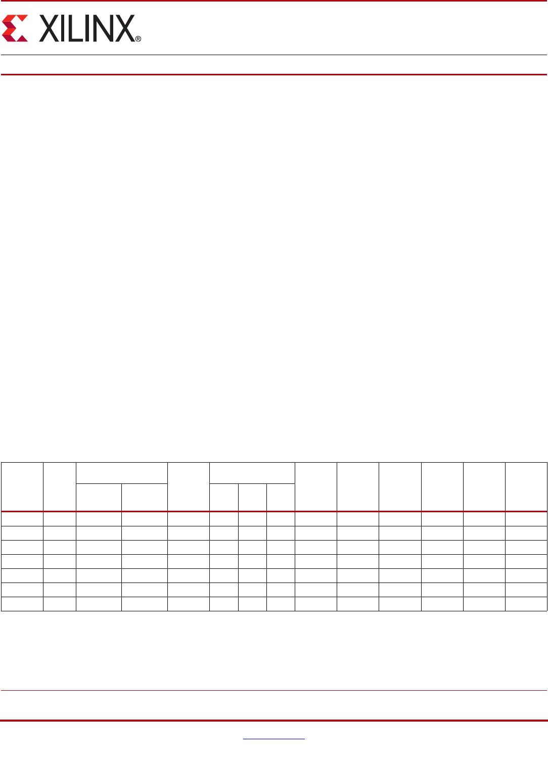
Table 1: XA Artix-7 FPGA Device-Feature Table
Device
Logic
Cells
Configurable Logic
Blocks (CLBs)
DSP48E1
Slices
(2)
Block RAM Blocks
(3)
CMTs
(4)
PCIe
(5)
GTPs
XADC
Blocks
Total I/O
Banks
(6)
Max User
I/O
(7)
Slices
(1)
Max
Distributed
RAM (Kb)
18 Kb 36 Kb
Max
(Kb)
XA7A12T12,8002,00017140402072031213150
XA7A15T16,6402,60020045502590051415210
XA7A25T23,3603,6503138090451,62031413150
XA7A35T33,2805,20040090100501,80051415210
XA7A50T52,1608,150600120150752,70051415210
XA7A75T75,52011,8008921802101053,78061416285
XA7A100T101,44015,8501,1882402701354,86061416285
Notes:
1. Each 7 series FPGA slice contains four LUTs and eight flip-flops; only some slices can use their LUTs as distributed RAM or SRLs.
2. Each DSP slice contains a pre-adder, a 25 x 18 multiplier, an adder, and an accumulator.
3. Block RAMs are fundamentally 36 Kb in size; each block can also be used as two independent 18 Kb blocks.
4. Each CMT contains one MMCM and one PLL.
5. XA Artix-7 FPGA Interface Blocks for PCI Express support up to x4 Gen 2.
6. Does not include configuration Bank 0.
7. This number does not include GTP transceivers.
XA Artix-7 FPGAs Data Sheet: Overview
DS197 (v1.2) February 23, 2017 www.xilinx.com
Product Specification 2
CLBs, Slices, and LUTs
Some key features of the CLB architecture include:
Real 6-input look-up tables (LUTs)
Memory capability within the LUT
Register and shift register functionality
The LUTs in 7 series FPGAs can be configured as either one 6-input LUT (64-bit ROMs) with one output, or as two 5-input
LUTs (32-bit ROMs) with separate outputs but common addresses or logic inputs. Each LUT output can optionally be
registered in a flip-flop. Four such LUTs and their eight flip-flops as well as multiplexers and arithmetic carry logic form a
slice, and two slices form a configurable logic block (CLB). Four of the eight flip-flops per slice (one per LUT) can optionally
be configured as latches.
Between 25–50% of all slices can also use their LUTs as distributed 64-bit RAM or as 32-bit shift registers (SRL32) or as two
SRL16s. Modern synthesis tools take advantage of these highly efficient logic, arithmetic, and memory features.
Clock Management
Some of the key highlights of the clock management architecture include:
High-speed buffers and routing for low-skew clock distribution
Frequency synthesis and phase shifting
Low-jitter clock generation and jitter filtering
Each XA Artix-7 FPGA has three to six clock management tiles (CMTs), each consisting of one mixed-mode clock manager
(MMCM) and one phase-locked loop (PLL).
Mixed-Mode Clock Manager and Phase-Locked Loop
The MMCM and PLL share many characteristics. Both can serve as a frequency synthesizer for a wide range of frequencies
and as a jitter filter for incoming clocks. At the center of both components is a voltage-controlled oscillator (VCO), which
speeds up and slows down depending on the input voltage it receives from the phase frequency detector (PFD).
There are three sets of programmable frequency dividers: D, M, and O. The pre-divider D (programmable by configuration
and afterwards via DRP) reduces the input frequency and feeds one input of the traditional PLL phase/frequency
comparator. The feedback divider M (programmable by configuration and afterwards via DRP) acts as a multiplier because
it divides the VCO output frequency before feeding the other input of the phase comparator. D and M must be chosen
appropriately to keep the VCO within its specified frequency range. The VCO has eight equally-spaced output phases
Table 2: XA Artix-7 FPGA Device-Package Combinations and Maximum I/Os
Package
(1)
CPG236 CSG324 CSG325 FGG484
Size (mm) 10 x 10 15 x 15 15 x 15 23 x 23
Ball Pitch (mm) 0.5 0.8 0.8 1.0
Device GTP
I/O
GTP
I/O
GTP
I/O
GTP
I/O
HR
(2)
HR
(2)
HR
(2)
HR
(2)
XA7A12T 2 106 2150
XA7A15T 2 106 0 210 4 150
XA7A25T 2 106 4150
XA7A35T 2 106 0 210 4 150
XA7A50T 2 106 0 210 4 150
XA7A75T 0 210 4 285
XA7A100T
0 210 4 285
Notes:
1. All packages listed are Pb-free.
2. HR = High Range I/O with support for I/O voltage from 1.2V to 3.3V.
XA Artix-7 FPGAs Data Sheet: Overview
DS197 (v1.2) February 23, 2017 www.xilinx.com
Product Specification 3
(0°, 45°, 90°, 135°, 180°, 225°, 270°, and 315°). Each can be selected to drive one of the output dividers (six for the PLL,
O0 to O5, and seven for the MMCM, O0 to O6), each programmable by configuration to divide by any integer from 1 to 128.
The MMCM and PLL have three input-jitter filter options: low bandwidth, high bandwidth, or optimized mode. Low-bandwidth
mode has the best jitter attenuation but not the smallest phase offset. High-bandwidth mode has the best phase offset, but
not the best jitter attenuation. Optimized mode allows the tools to find the best setting.
MMCM Additional Programmable Features
The MMCM can have a fractional counter in either the feedback path (acting as a multiplier) or in one output path. Fractional
counters allow non-integer increments of
1
/8 and can thus increase frequency synthesis capabilities by a factor of 8.
The MMCM can also provide fixed or dynamic phase shift in small increments that depend on the VCO frequency. At
1440 MHz, the phase-shift timing increment is 12.5 ps.
Clock Distribution
Each 7 series FPGA provides six different types of clock lines (BUFG, BUFR, BUFIO, BUFH, BUFMR, and the high-
performance clock) to address the different clocking requirements of high fanout, short propagation delay, and extremely low
skew.
Global Clock Lines
In each 7 series FPGA, 32 global clock lines have the highest fanout and can reach every flip-flop clock, clock enable, and
set/reset, as well as many logic inputs. There are 12 global clock lines within any clock region driven by the horizontal clock
buffers (BUFH). Each BUFH can be independently enabled/disabled, allowing for clocks to be turned off within a region,
thereby offering fine-grain control over which clock regions consume power. Global clock lines can be driven by global clock
buffers, which can also perform glitchless clock multiplexing and clock enable functions. Global clocks are often driven from
the CMT, which can completely eliminate the basic clock distribution delay.
Regional Clocks
Regional clocks can drive all clock destinations in their region. A region is an area that is 50 I/O and 50 CLB high and half
the chip wide. XA Artix-7 FPGAs have between six and eight regions. There are four regional clock tracks in every region.
Each regional clock buffer can be driven from any of four clock-capable input pins, and its frequency can optionally be
divided by any integer from 1 to 8.
I/O Clocks
I/O clocks are especially fast and serve only I/O logic and serializer/deserializer (SerDes) circuits, as described in the
I/O Logic section. The 7 series devices have a direct connection from the MMCM to the I/O for low-jitter, high-performance
interfaces.
Block RAM
Some of the key features of the block RAM include:
Dual-port 36 Kb block RAM with port widths of up to 72
Programmable FIFO logic
Built-in optional error correction circuitry
Every XA Artix-7 FPGA has between 20 and 135 dual-port block RAMs, each storing 36 Kb. Each block RAM has two
completely independent ports that share nothing but the stored data.
Synchronous Operation
Each memory access, read or write, is controlled by the clock. All inputs, data, address, clock enables, and write enables are
registered. Nothing happens without a clock. The input address is always clocked, retaining data until the next operation. An
optional output data pipeline register allows higher clock rates at the cost of an extra cycle of latency.

XA7A35T-1CSG325Q

Mfr. #:
Manufacturer:
Xilinx
Description:
FPGA - Field Programmable Gate Array XA7A35T-1CSG325Q
Lifecycle:
New from this manufacturer.
Delivery:
DHL FedEx Ups TNT EMS
Payment:
T/T Paypal Visa MoneyGram Western Union