VS-MBRB4045CTR-M3

VS-MBRB4045CTHM3, VS-MBR4045CT-1HM3
www.vishay.com
Vishay Semiconductors
Revision: 06-Mar-14
1
Document Number: 94721
For technical questions within your region: DiodesAmericas@vishay.com
, DiodesAsia@vishay.com, DiodesEurope@vishay.com
THIS DOCUMENT IS SUBJECT TO CHANGE WITHOUT NOTICE. THE PRODUCTS DESCRIBED HEREIN AND THIS DOCUMENT
ARE SUBJECT TO SPECIFIC DISCLAIMERS, SET FORTH AT www.vishay.com/doc?91000
Schottky Rectifier, 2 x 20 A
FEATURES
150 °C T
J
operation
Low forward voltage drop
High frequency operation
High purity, high temperature epoxy
encapsulation for enhanced mechanical
strength and moisture resistance
Guard ring for enhanced ruggedness and long
term reliability
Meets MSL level 1, per J-STD-020, LF maximum peak of
260 °C
• AEC-Q101 qualified, meets JESD 201 class 1A whisker
test
Material categorization: For definitions of compliance
please see www.vishay.com/doc?99912
DESCRIPTION
The center tap Schottky rectifier has been optimized for low
reverse leakage at high temperature. The proprietary barrier
technology allows for reliable operation up to 150 °C
junction temperature. Typical applications are in switching
power supplies, converters, freewheeling diodes, and
reverse battery protection.
PRODUCT SUMMARY
Package TO-263AB (D
2
PAK), TO-262AA
I
F(AV)
2 x 20 A
V
R
45 V
V
F
at I
F
0.58 V
I
RM
max. 95 mA at 125 °C
T
J
max. 150 °C
Diode variation Common cathode
E
AS
20 mJ
VS-MBRB4045CTHM3
D
2
PAK
TO-262
VS-MBR4045CT-1HM3
Base
common
cathode
Anode Anode
Common
cathode
1
3
2
2
Base
common
cathode
Anode Anode
Common
cathode
1
3
2
2
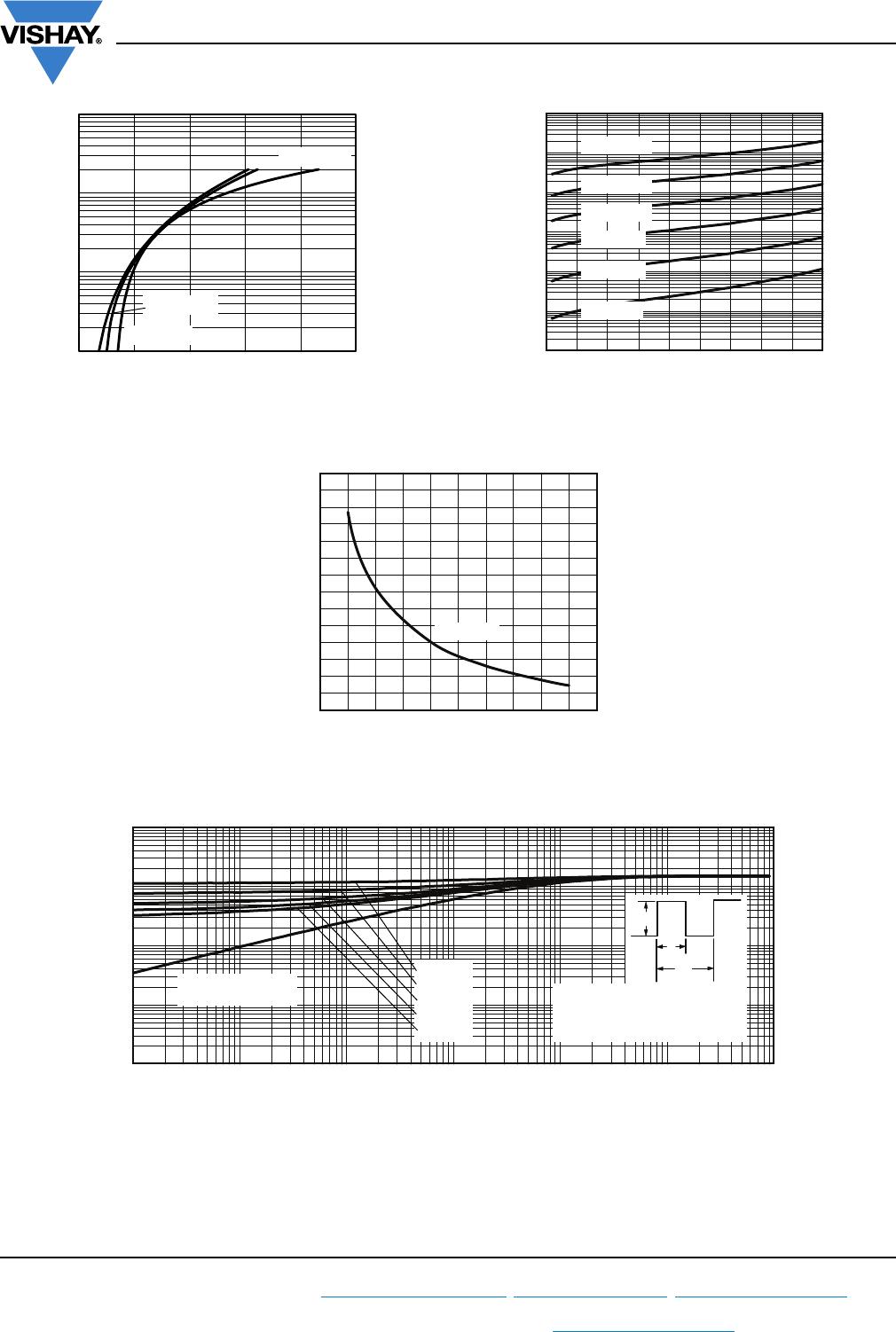
MAJOR RATINGS AND CHARACTERISTICS
SYMBOL CHARACTERISTICS VALUES UNITS
I
F(AV)
Rectangular waveform (per device) 40
A
I
FRM
T
C
= 117 °C (per leg) 40
V
RRM
45 V
I
FSM
t
p
= 5 μs sine 900 A
V
F
20 A
pk
, T
J
= 125 °C 0.58 V
T
J
Range -65 to 150 °C
VOLTAGE RATINGS
PARAMETER SYMBOL
VS-MBRB4045CTHM3
VS-MBR4045CT-1HM3
UNITS
Maximum DC reverse voltage V
R
45 V
Maximum working peak reverse voltage V
RWM
ABSOLUTE MAXIMUM RATINGS
PARAMETER SYMBOL TEST CONDITIONS VALUES UNITS
Maximum average
forward current
per leg
I
F(AV)
T
C
= 118 °C, rated V
R
20
A
per device 40
Peak repetitive forward current per leg I
FRM
Rated V
R
, square wave, 20 kHz, T
C
= 117 °C 40
Maximum peak one cycle non-repetitive
peak surge current per leg
I
FSM
5 μs sine or 3 μs rect. pulse Following any rated
load condition and with
rated V
RRM
applied
900
10 ms sine or 6 ms rect. pulse 210
Non-repetitive avalanche energy per leg E
AS
T
J
= 25 °C, I
AS
= 3 A, L = 4.4 mH 20 mJ
Repetitive avalanche current per leg I
AR
Current decaying linearly to zero in 1 μs
Frequency limited by T
J
maximum V
A
= 1.5 x V
R
typical
3A
VS-MBRB4045CTHM3, VS-MBR4045CT-1HM3
www.vishay.com
Vishay Semiconductors
Revision: 06-Mar-14
2
Document Number: 94721
For technical questions within your region: DiodesAmericas@vishay.com
, DiodesAsia@vishay.com, DiodesEurope@vishay.com
THIS DOCUMENT IS SUBJECT TO CHANGE WITHOUT NOTICE. THE PRODUCTS DESCRIBED HEREIN AND THIS DOCUMENT
ARE SUBJECT TO SPECIFIC DISCLAIMERS, SET FORTH AT www.vishay.com/doc?91000
Note
(1)
Pulse width < 300 μs, duty cycle < 2 %
ELECTRICAL SPECIFICATIONS
PARAMETER SYMBOL TEST CONDITIONS VALUES UNITS
Maximum forward voltage drop V
FM
(1)
20 A
T
J
= 25 °C
0.60
V
40 A 0.80
20 A
T
J
= 125 °C
0.58
40 A 0.80
Maximum instantaneous
reverse current
I
RM
(1)
T
J
= 25 °C
Rated DC voltage
1
mAT
J
= 100 °C 50
T
J
= 125 °C 95
Maximum junction capacitance C
T
V
R
= 5 V
DC
(test signal range 100 kHz to 1 MHz), 25 °C 900 pF
Typical series inductance L
S
Measured from top of terminal to mounting plane 8.0 nH
Maximum voltage rate of change dV/dt Rated V
R
10 000 V/μs
THERMAL - MECHANICAL SPECIFICATIONS
PARAMETER SYMBOL TEST CONDITIONS VALUES UNITS
Maximum junction temperature range T
J
-65 to 150
°C
Maximum storage temperature range T
Stg
-65 to 175
Maximum thermal resistance,
junction to case per leg
R
thJC
DC operation 1.5
°C/W
Typical thermal resistance,
case to heatsink
R
thCS
Mounting surface, smooth and greased
(Only for TO-220)
0.50
Maximum thermal resistance,
junction to ambient
R
thJA
DC operation
(For D
2
PAK and TO-262)
50
Approximate weight
2g
0.07 oz.
Mounting torque
minimum
Non-lubricated threads
6 (5)
kgf · cm
(lbf · in)
maximum 12 (10)
Marking device
Case style D
2
PAK MBRB4045CTH
Case style TO-262 MBR4045CT-1H
VS-MBRB4045CTHM3, VS-MBR4045CT-1HM3
www.vishay.com
Vishay Semiconductors
Revision: 06-Mar-14
3
Document Number: 94721
For technical questions within your region: DiodesAmericas@vishay.com
, DiodesAsia@vishay.com, DiodesEurope@vishay.com
THIS DOCUMENT IS SUBJECT TO CHANGE WITHOUT NOTICE. THE PRODUCTS DESCRIBED HEREIN AND THIS DOCUMENT
ARE SUBJECT TO SPECIFIC DISCLAIMERS, SET FORTH AT www.vishay.com/doc?91000
Fig. 1 - Maximum Forward Voltage Drop Characteristics
(Per Leg)
Fig. 2 - Typical Values of Reverse Current vs.
Reverse Voltage (Per Leg)
Fig. 3 - Typical Junction Capacitance vs. Reverse Voltage (Per Leg)
Fig. 4 - Maximum Thermal Impedance Z
thJC
Characteristics (Per Leg)
1
10
100
1000
0 0.5 1.0 1.5 2.0 2.5
I
F
- Instantaneous Forward Current (A)
V
F
- Forward Voltage Drop (V)
T
J
= 125 °C
T
J
= 25 °C
T
J
= 175 °C
0.001
1
10
100
0.1
0.01
1000
I
R
- Reverse Current (mA)
V
R
- Reverse Voltage (V)
1051520
40
45
25 30 35
0
T
J
= 150 °C
T
J
= 125 °C
T
J
= 100 °C
T
J
= 75 °C
T
J
= 50 °C
T
J
= 25 °C
200
300
600
400
700
800
900
500
C
T
- Junction Capacitance (pF)
V
R
- Reverse Voltage (V)
10 20
40
30
0
50
T
J
= 25 °C
0.01
0.1
1
10
0.00001 0.0001 0.001 0.01 0.1 1
t
1
- Rectangular Pulse Duration (s)
Z
thJC
- Thermal Impedance (°C/W)
10
Single pulse
(thermal resistance)
D = 0.75
D = 0.50
D = 0.33
D = 0.25
D = 0.20
P
DM
t
1
t
2
Notes:
1. Duty factor D = t
1
/t
2
2. Peak T
J
= P
DM
x Z
thJC
+ T
C
0.001

VS-MBRB4045CTR-M3

Mfr. #:
Manufacturer:
Vishay Semiconductors
Description:
Schottky Diodes & Rectifiers Schottky - D2PAK-e3
Lifecycle:
New from this manufacturer.
Delivery:
DHL FedEx Ups TNT EMS
Payment:
T/T Paypal Visa MoneyGram Western Union