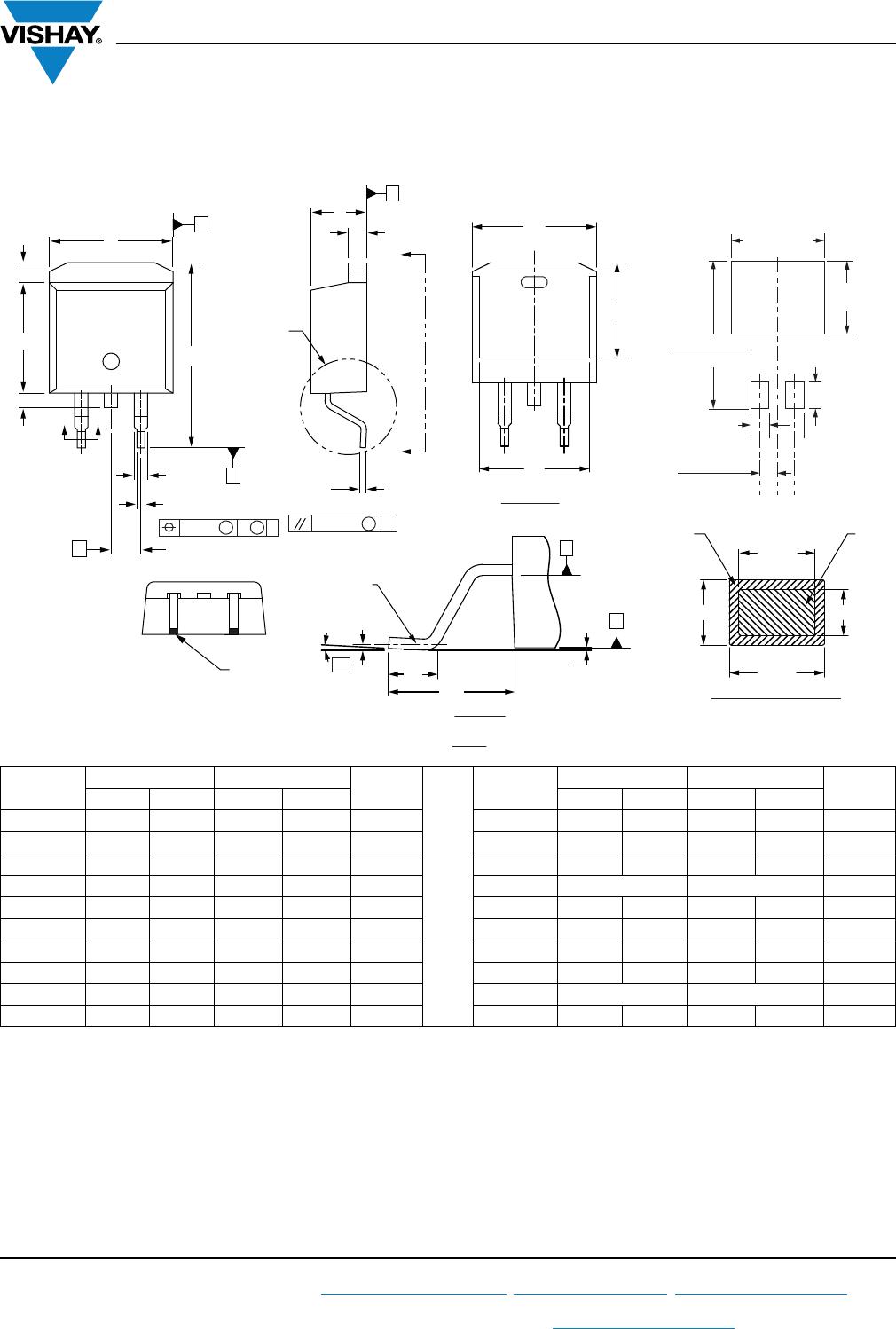
VS-MBRB4045CTR-M3

VS-MBRB4045CTHM3, VS-MBR4045CT-1HM3
www.vishay.com
Vishay Semiconductors
Revision: 06-Mar-14
4
Document Number: 94721
For technical questions within your region: DiodesAmericas@vishay.com
, DiodesAsia@vishay.com, DiodesEurope@vishay.com
THIS DOCUMENT IS SUBJECT TO CHANGE WITHOUT NOTICE. THE PRODUCTS DESCRIBED HEREIN AND THIS DOCUMENT
ARE SUBJECT TO SPECIFIC DISCLAIMERS, SET FORTH AT www.vishay.com/doc?91000
Fig. 5 - Maximum Allowable Case Temperature vs.
Average Forward Current
Fig. 6 - Forward Power Loss Characteristics
Fig. 7 - Maximum Non-Repetitive Surge Current (Per Leg)
Note
(1)
Formula used: T
C
= T
J
- (Pd + Pd
REV
) x R
thJC
;
Pd = Forward power loss = I
F(AV)
x V
FM
at (I
F(AV)
/D) (see fig. 6);
Pd
REV
= Inverse power loss = V
R1
x I
R
(1 - D); I
R
at V
R1
= Rated V
R
80
90
100
110
120
130
140
150
160
0 5 10 15 20 25 30
Allowable Case Temperature (°C)
I
F(AV)
- Average Forward Current (A)
Square wave (D = 0.50)
80 % rated V
R
applied
See note
(1)
DC
0
5
10
15
20
0 5 10 15 20 25 30
Average Power Loss (W)
I
F(AV)
- Average Forward Current (A)
D = 0.20
D = 0.25
D = 0.33
D = 0.50
D = 0.75
DC
RMS limit
100
1000
I
FSM
- Non-Repetitive Surge Current (A)
t
p
- Square Wave Pulse Duration (µs)
100 1000
10 000
10
At any rated load condition
and with rated V
RRM
applied
following surge
VS-MBRB4045CTHM3, VS-MBR4045CT-1HM3
www.vishay.com
Vishay Semiconductors
Revision: 06-Mar-14
5
Document Number: 94721
For technical questions within your region: DiodesAmericas@vishay.com
, DiodesAsia@vishay.com, DiodesEurope@vishay.com
THIS DOCUMENT IS SUBJECT TO CHANGE WITHOUT NOTICE. THE PRODUCTS DESCRIBED HEREIN AND THIS DOCUMENT
ARE SUBJECT TO SPECIFIC DISCLAIMERS, SET FORTH AT www.vishay.com/doc?91000
ORDERING INFORMATION TABLE
ORDERING INFORMATION (Example)
PREFERRED P/N QUANTITY PER T/R MINIMUM ORDER QUANTITY PACKAGING DESCRIPTION
VS-MBRB4045CTHM3 50 1000 Antistatic plastic tube
VS-MBR4045CT-1HM3 50 1000 Antistatic plastic tube
VS-MBRB4045CTLHM3 800 800 13" diameter reel
VS-MBRB4045CTRHM3 800 800 13" diameter reel
LINKS TO RELATED DOCUMENTS
Dimensions
TO-263AB (D
2
PAK) www.vishay.com/doc?95046
TO-262AA www.vishay.com/doc?95419
Part marking information
TO-263AB (D
2
PAK) www.vishay.com/doc?95444
TO-262AA www.vishay.com/doc?95443
Packaging information TO-263AB (D
2
PAK) www.vishay.com/doc?95032
2
- Essential part number
3 -
4
- Current rating (40 = 40 A)
5 -
8 - None = Tube
L = Tape and reel (left oriented - for D
2
PAK only)
Voltage rating (45 = 45 V)
7 -
None = D
2
PAK
-1 = TO-262
B = D
2
PAK
None = TO-262
7
7
None
= -1
6
-
CT = Essential part number
3
= B
3
None
R = Tape and reel (right oriented - for D
2
PAK only)
1 - Vishay Semiconductors product
Device code
51 32 4 6 7 8 9 10
VS- MBR B 40 45 CT -1 RL H M3
10
- Environmental digit:
M3 = Halogen-free, RoHS-compliant and termination lead (Pb)-free
9
- H = AEC-Q101 qualified
Outline Dimensions
www.vishay.com
Vishay Semiconductors
Revision: 08-Jul-15
1
Document Number: 95046
For technical questions within your region: DiodesAmericas@vishay.com
, DiodesAsia@vishay.com, DiodesEurope@vishay.com
THIS DOCUMENT IS SUBJECT TO CHANGE WITHOUT NOTICE. THE PRODUCTS DESCRIBED HEREIN AND THIS DOCUMENT
ARE SUBJECT TO SPECIFIC DISCLAIMERS, SET FORTH AT www.vishay.com/doc?91000
D
2
PAK
DIMENSIONS in millimeters and inches
Notes
(1)
Dimensioning and tolerancing per ASME Y14.5 M-1994
(2)
Dimension D and E do not include mold flash. Mold flash shall not exceed 0.127 mm (0.005") per side. These dimensions are measured at
the outmost extremes of the plastic body
(3)
Thermal pad contour optional within dimension E, L1, D1 and E1
(4)
Dimension b1 and c1 apply to base metal only
(5)
Datum A and B to be determined at datum plane H
(6)
Controlling dimension: inch
(7)
Outline conforms to JEDEC
®
outline TO-263AB
SYMBOL
MILLIMETERS INCHES
NOTES SYMBOL
MILLIMETERS INCHES
NOTES
MIN. MAX. MIN. MAX. MIN. MAX. MIN. MAX.
A 4.06 4.83 0.160 0.190 D1 6.86 8.00 0.270 0.315 3
A1 0.00 0.254 0.000 0.010 E 9.65 10.67 0.380 0.420 2, 3
b 0.51 0.99 0.020 0.039 E1 7.90 8.80 0.311 0.346 3
b1 0.51 0.89 0.020 0.035 4 e 2.54 BSC 0.100 BSC
b2 1.14 1.78 0.045 0.070 H 14.61 15.88 0.575 0.625
b3 1.14 1.73 0.045 0.068 4 L 1.78 2.79 0.070 0.110
c 0.38 0.74 0.015 0.029 L1 - 1.65 - 0.066 3
c1 0.38 0.58 0.015 0.023 4 L2 1.27 1.78 0.050 0.070
c2 1.14 1.65 0.045 0.065 L3 0.25 BSC 0.010 BSC
D 8.51 9.65 0.335 0.380 2 L4 4.78 5.28 0.188 0.208
c
B
Detail A
c2
AA
A
± 0.004
B
M
A
Lead tip
(3)
(3)
View A - A
(E)
(D1)
E1
B
H
A1
Detail “A”
Rotated 90 °CW
Scale: 8:1
L
Gauge
plane
0° to 8°
L3
L4
Seating
plane
Section B - B and C - C
Scale: None
(4)
(4)
(b, b2)
b1, b3
(c)
c1
Base
Metal
Plating
Conforms to JEDEC
®
outline D
2
PAK (SMD-220)
132
D
C
A
L2
E
(2)(3)
(2)
4
H
BB
2 x b
2 x b2
L1
0.010
A
B
M
M
(3)
e
2 x
Pad layout
MIN.
11.00
(0.43)
MIN.
9.65
(0.38)
MIN.
3.81
(0.15)
MIN.
2.32
(0.08)
17.90 (0.70)
15.00 (0.625)
2.64 (0.103)
2.41 (0.096)

VS-MBRB4045CTR-M3

Mfr. #:
Manufacturer:
Vishay Semiconductors
Description:
Schottky Diodes & Rectifiers Schottky - D2PAK-e3
Lifecycle:
New from this manufacturer.
Delivery:
DHL FedEx Ups TNT EMS
Payment:
T/T Paypal Visa MoneyGram Western Union