FCB199N65S3
www.onsemi.com
2
ABSOLUTE MAXIMUM RATINGS (T
C
= 25°C, Unless otherwise specified)
Symbol
Parameter Value Unit
V
DSS
Drain to Source Voltage 650 V
V
GSS
Gate to Source Voltage
DC ±30 V
AC (f > 1 Hz) ±30 V
I
D
Drain Current
Continuous (T
C
= 25°C) 14
A
Continuous (T
C
= 100°C) 9
I
DM
Drain Current Pulsed (Note 1) 35 A
E
AS
Single Pulsed Avalanche Energy (Note 2) 76 mJ
I
AS
Avalanche Current (Note 1) 2.5 A
E
AR
Repetitive Avalanche Energy (Note 1) 0.98 mJ
dv/dt
MOSFET dv/dt 100
V/ns
Peak Diode Recovery dv/dt (Note 3) 20
P
D
Power Dissipation
(T
C
= 25°C) 98 W
Derate Above 25°C 0.79 W/°C
T
J
, T
STG
Operating and Storage Temperature Range −55 to +150 °C
T
L
Maximum Lead Temperature for Soldering, 1/8″ from Case for 5 s 300 °C
Stresses exceeding those listed in the Maximum Ratings table may damage the device. If any of these limits are exceeded, device functionality
should not be assumed, damage may occur and reliability may be affected.
1. Repetitive rating: pulse-width limited by maximum junction temperature.
2. I
AS
= 2.5 A, R
G
= 25 W, starting T
J
= 25°C.
3. I
SD
≤ 7 A, di/dt ≤ 200 A/ms, V
DD
≤ 400 V, starting T
J
= 25°C.
THERMAL CHARACTERISTICS
Symbol Parameter Value Unit
R
q
JC
Thermal Resistance, Junction to Case, Max. 1.27 _C/W
Thermal Resistance, Junction to Ambient, Max. (Note 4) 40
4. Device on 1 in
2
pad 2 oz copper pad on 1.5 x 1.5 in. board of FR−4 material.
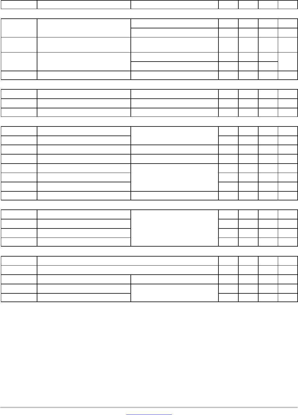
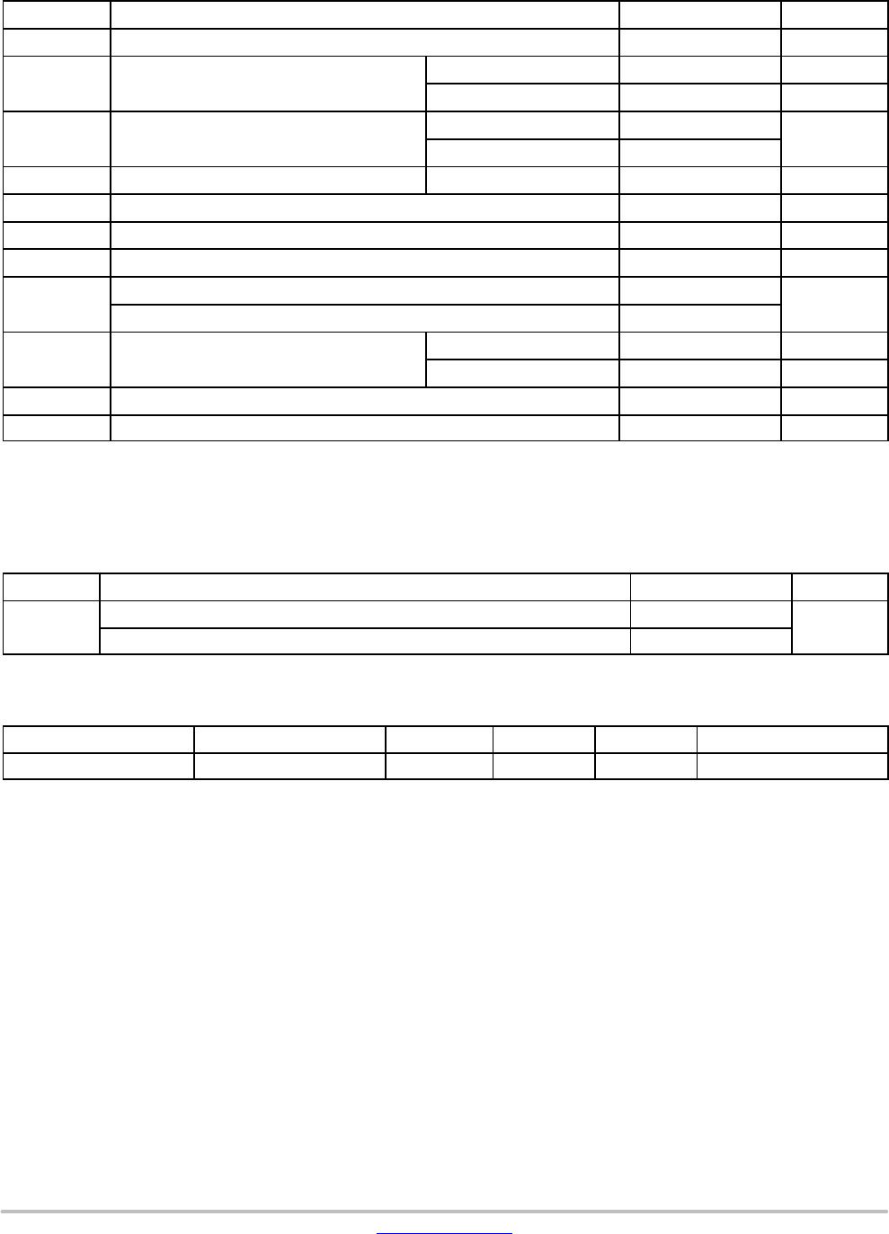
PACKAGE MARKING AND ORDERING INFORMATION
Part Number Top Marking Package Reel Size Tape Width Shipping
†
FCB199N65S3 FCB199N65S3 D
2
−PAK 330 mm 24 mm 800 / Tape & Reel
†For information on tape and reel specifications, including part orientation and tape sizes, please refer to our Tape and Reel Packaging
Specifications Brochure, BRD8011/D.