I/O
14-pin PDIP/SOIC/TSSOP
16-pin UQFN
ADC
Reference
Comparator
NCO
DAC
DSM
Timers
CCP
PWM
CWG
MSSP
ZCD
EUSART
CLC
CLKR
Interrupts
Pull-up
Basic
ADCGRDB C2OUT CCP2OUT PWM7OUT
CWG1B
CWG2B
SCK1
SCK2
CK1
(3)
CLC2OUT
CCP3OUT
CWG1C
CWG2C
SCL1
(3)
SCL2
(3)
TX1 CLC3OUT
CCP4OUT
CWG1D
CWG2D
SDA1
(3)
SDA2
(3)
CLC4OUT
Note: 
1. This is a PPS re-mappable input signal. The input function may be moved from the default location
shown to one of several other PORTx pins.
2. All digital output signals shown in these rows are PPS re-mappable. These signals may be mapped to
output onto one of several PORTx pin options.
3. This is a bidirectional signal. For normal module operation, the firmware should map this signal to the
same pin in both the PPS input and PPS output registers.
4. These pins are configured for I
2
C logic levels. PPS assignments to the other pins will operate, but input
logic levels will be standard TTL/ST as selected by the INLVL register, instead of the I
2
C specific or
SMBUS input buffer thresholds.
5. MSSP2 is not available on the PIC16(L)F18424 or PIC16(L)F18444 devices.
2 20-Pin Allocation Table
I/O
20-pin PDIP/SOIC/TSSOP
20-pin UQFN
ADC
Reference
Comparator
NCO
DAC
DSM
Timers
CCP
PWM
CWG
MSSP
ZCD
EUSART
CLC
CLKR
Interrupts
Pull-up
Basic
RA0 19 16 ANA0 C1IN0+ DAC1OUT1 IOCA0 Y
ICDDAT/
ICSPDAT
RA1 18 15 ANA1
ADCVREF
+
C1IN0-
C2IN0-
DAC1VREF
+
MDSRC
(1)
SS2
(1)
IOCA1 Y
ICDCLK/
ICSPCLK
RA2 17 14 ANA2 ADCVREF- DAC1VREF- T0CKI
(1)
CWG1IN
(1)
CWG2IN
(1)
ZCD1 CLCIN0
(1)
IOCA2 Y INT0
(1)
RA3 4 1 IOCA3 Y
MCLR
V
PP
RA4 3 20 ANA4
T1G
(1)
CCP4IN
(1)
IOCA4 Y
CLKOUT
PIC16(L)F184XX
© 2017 Microchip Technology Inc.
Product Brief
DS40001894B-page 10
I/O
20-pin PDIP/SOIC/TSSOP
20-pin UQFN
ADC
Reference
Comparator
NCO
DAC
DSM
Timers
CCP
PWM
CWG
MSSP
ZCD
EUSART
CLC
CLKR
Interrupts
Pull-up
Basic
SMT1WIN
(1)
SOSCO
OSC2
RA5 2 19 ANA5
T1CKI
(1)
T2IN
(1)
SMT1SIG
(1)
IOCA5 Y
CLKIN
SOSCI
OSC1
RB4 13 10 ANB4 T5G
(1)
SDI1
(1)
SDA1
(1,3,4)
CLCIN2
(1)
IOCB4 Y
RB5 12 9 ANB5 CCP3IN
(1)
SCK2
(1,5)
SCL2
(1,3,4,5)
RX1
(1)
DT1
(1,3)
CLCIN3
(1)
IOCB5 Y
RB6 11 8 ANB6
SCK1
(1)
SCL1
(1,3,4)
IOCB6 Y
RB7 10 7 ANB7 T6IN
(1)
SDI2
(1,5)
SDA2
(1,3,4,5)
CK1
(1,3)
IOCB7 Y
RC0 16 13 ANC0 C2IN0+
T3CKI
(1)
T3G
(1)
IOCC0 Y
RC1 15 12 ANC1
C1IN1-
C2IN1-
IOCC1 Y
RC2 14 11
ANC2
ADACT
(1)
C1IN2-
C2IN2-
MDCARL
(1)
T5CKI
(1)
IOCC2 Y
RC3 7 4 ANC3
C1IN3-
C2IN3-
CCP2IN
(1)
CLCIN1
(1)
IOCC3 Y
RC4 6 3 ANC4 IOCC4 Y
RC5 5 2 ANC5 MDCARH
(1)
T4IN
(1)
CCP1IN
(1)
IOCC5 Y
RC6 8 5 ANC6 SS1
(1)
IOCC6 Y
RC7 9 6 ANC7 IOCC7 Y
V
DD
1 18 V
DD
V
SS
20 17 V
SS
OUT
(2)
ADCGRDA C1OUT NCO1OUT DSM1OUT TMR0OUT CCP1OUT PWM6OUT
CWG1A
CWG2A
SDO1
SDO2
DT1
(3)
CLC1OUT CLKR
ADCGRDB C2OUT CCP2OUT PWM7OUT
CWG1B
CWG2B
SCK1
SCK2
CK1
(3)
CLC2OUT
PIC16(L)F184XX
© 2017 Microchip Technology Inc.
Product Brief
DS40001894B-page 11
I/O
20-pin PDIP/SOIC/TSSOP
20-pin UQFN
ADC
Reference
Comparator
NCO
DAC
DSM
Timers
CCP
PWM
CWG
MSSP
ZCD
EUSART
CLC
CLKR
Interrupts
Pull-up
Basic
CCP3OUT
CWG1C
CWG2C
SCL1
(3)
SCL2
(3)
TX1 CLC3OUT
CCP4OUT
CWG1D
CWG2D
SDA1
(3)
SDA2
(3)
CLC4OUT
Note: 
1. This is a PPS re-mappable input signal. The input function may be moved from the default location
shown to one of several other PORTx pins.
2. All digital output signals shown in these rows are PPS re-mappable. These signals may be mapped to
output onto one of several PORTx pin options.
3. This is a bidirectional signal. For normal module operation, the firmware should map this signal to the
same pin in both the PPS input and PPS output registers.
4. These pins are configured for I
2
C logic levels. PPS assignments to the other pins will operate, but input
logic levels will be standard TTL/ST as selected by the INLVL register, instead of the I
2
C specific or
SMBUS input buffer thresholds.
5. MSSP2 is not available on the PIC16(L)F18424 or PIC16(L)F18444 devices.
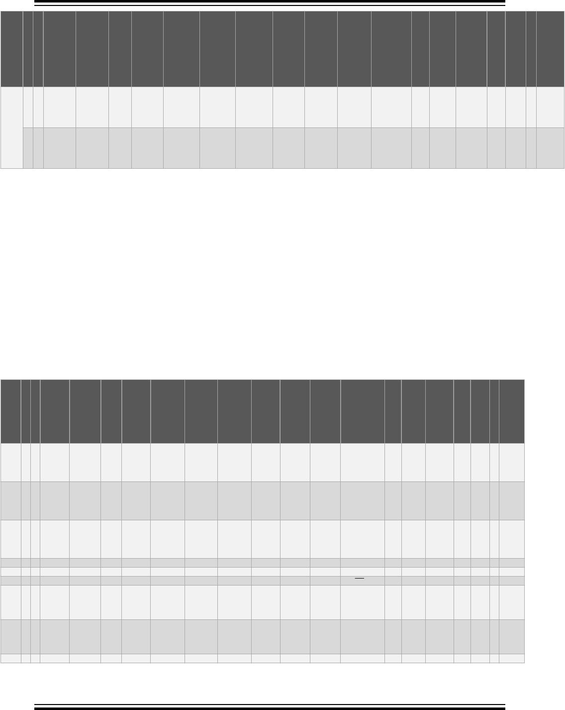
3 28-Pin Allocation Table
I/O
28-pin PDIP/SOIC/TSSOP
28-pin UQFN
ADC
Reference
Comparator
NCO
DAC
DSM
Timers
CCP
PWM
CWG
MSSP
ZCD
EUSART
CLC
CLKR
Interrupts
Pull-up
Basic
RA0 2 27 ANA0
C1IN0-
C2IN0-
CLCIN0
(1)
IOCA0 Y
RA1 3 28 ANA1
C1IN1-
C2IN1-
CLCIN1
(1)
IOCA1 Y
RA2 4 1 ANA2 ADCVREF-
C1IN0+
C2IN0+
DAC1VREF-
DAC1OUT1
IOCA2 Y
RA3 5 2 ANA3 ADCVREF+ C1IN1+ DAC1VREF+ MDCARL
(1)
IOCA3 Y
RA4 6 3 ANA4 MDCARH
(1)
T0CKI
(1)
CCP5IN
(1)
IOCA4 Y
RA5 7 4 ANA5 MDSRC
(1)
SS1
(1)
IOCA5 Y
RA6 10 7 ANA6 IOCA6 Y
OSC2
CLKOUT
RA7 9 6 ANA7 IOCA7 Y
OSC1
CLKIN
RB0 21 18 ANB0 C2IN1+ CCP4IN
(1)
CWG1IN
(1)
ZCD1 IOCB0 Y INT0
(1)
PIC16(L)F184XX
© 2017 Microchip Technology Inc.
Product Brief
DS40001894B-page 12

PIC16LF18424-I/P

Mfr. #:
Manufacturer:
Microchip Technology
Description:
8-bit Microcontrollers - MCU 7KB, 512B RAM, 2xPWMs, Comparator, DAC, 12-bit ADCC, CWG, EUSART, SPI/I2C
Lifecycle:
New from this manufacturer.
Delivery:
DHL FedEx Ups TNT EMS
Payment:
T/T Paypal Visa MoneyGram Western Union