PS9905 Chapt
R08DS0058EJ0100 Rev.1.00 Page 4 of 18
Jun 11, 2012
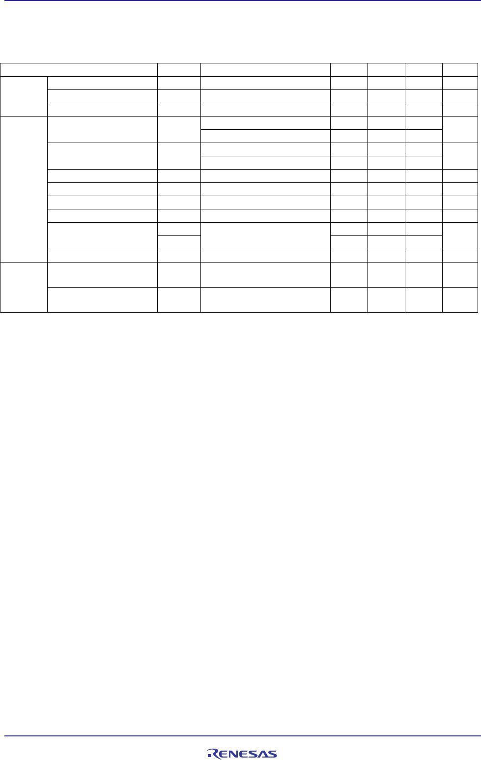
ORDERING INFORMATION
Part Number Order Number
Solder
Plating
Specification
Packing Style
Safety Standard
Approval
Application
Part
Number
*1
PS9905 PS9905-Y-AX 10 pcs (Tape 10 pcs cut)
PS9905-F3 PS9905-Y-F3-AX Embossed Tape 1 000
pcs/reel
Standard products
(UL, CSA, SEMKO
approved)
PS9905-V PS9905-Y-V-AX 10 pcs (Tape 10 pcs cut)
PS9905-V-F3 PS9905-Y-V-F3-AX Embossed Tape 1 000
Pb-Free
(Ni/Pd/Au)
pcs/reel
DIN EN60747-5-5
(VDE0884-5):
2011-11
approved (Option)
PS9905
Note: *1. For the application of the Safety Standard, following part number should be used.
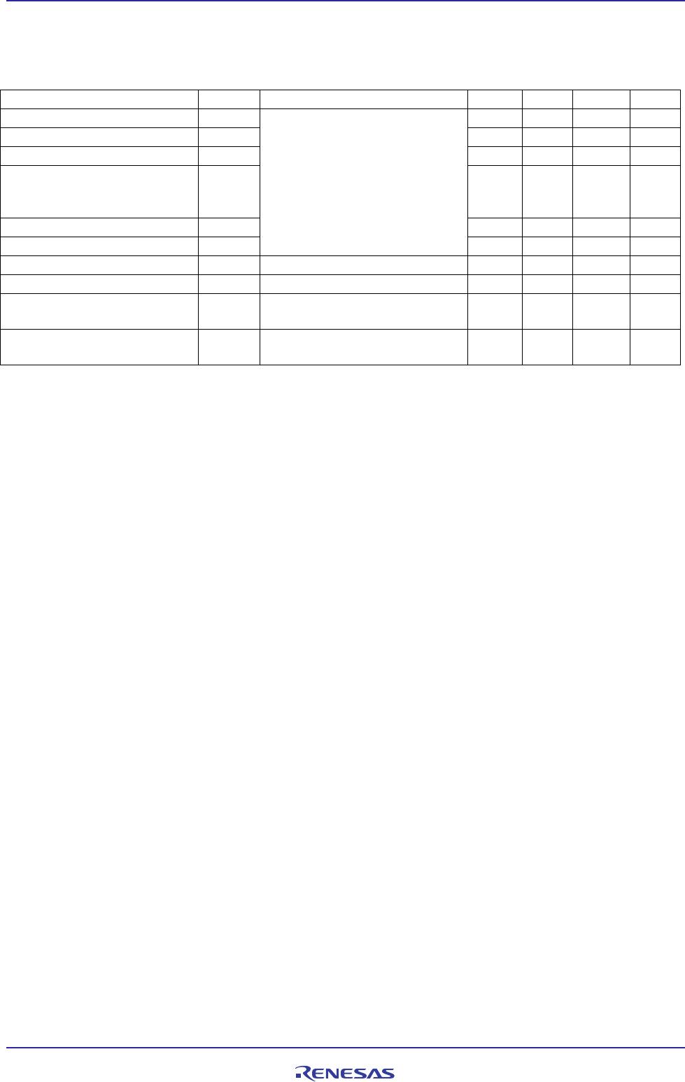
ABSOLUTE MAXIMUM RATINGS (T
A
= 25°C, unless otherwise specified)
Parameter Symbol Ratings Unit
Diode Forward Current I
F
25 mA
Peak Transient Forward
Current (Pulse Width < 1
μ
s)
I
F (TRAN)
1.0 A
Reverse Voltage V
R
5 V
Power Dissipation
*1, *6
P
D
45 mW
Detector
High Level Peak Output
Current
*2
I
OH (PEAK)
2.5 A
Low Level Peak Output
Current
*2
I
OL (PEAK)
2.5 A
Supply Voltage (V
CC
- V
EE
) 0 to 35 V
Output Voltage V
O
0 to V
CC
V
Power Dissipation
*3, *6
P
C
250 mW
Isolation Voltage
*4
BV 7 500 Vr.m.s.
Operating Frequency
*5
f 50 kHz
Operating Ambient Temperature T
A
40 to +110 °C
Storage Temperature T
stg
55 to +125 °C
Notes: *1. Derating to be set after 0.8 mW/°C at T
A
= 85°C or more.
*2. Maximum pulse width = 10
μ
s, Maximum duty cycle = 0.2 %
*3. Reduced to 5.2 mW/°C at T
A
= 85°C or more
*4. AC voltage for 1 minute at T
A
= 25°C, RH = 60% between input and output.
Pins 1-4 shorted together, 5-8 shorted together.
*5. I
OH (PEAK)
2.0 A ( 0.3
μ
s), I
OL (PEAK)
2.0 A ( 0.3
μ
s)
*6. Mounted on glass epoxy substrate of 75 mm × 115 mm × t1.5 mm
RECOMMENDED OPERATING CONDITIONS
Parameter Symbol MIN. TYP. MAX. Unit
Supply Voltage (V
CC
- V
EE
) 15 30 V
Forward Current (ON) I
F (ON)
10 12 14 mA
Forward Voltage (OFF) V
F (OFF)
2 0.8 V
Operating Ambient Temperature T
A
40 110 °C
<R>
<R>
PS9905 Chapt
R08DS0058EJ0100 Rev.1.00 Page 5 of 18
Jun 11, 2012
ELECTRICAL CHARACTERISTICS
(V
EE
= GND, unless otherwise specified and refer to RECOMMENDED OPERATING
CONDITIONS)
Parameter Symbol Conditions MIN. TYP.
*1
MAX. Unit
Diode Forward Voltage V
F
I
F
= 10 mA, T
A
= 25°C 1.3 1.56 1.8 V
Reverse Current I
R
V
R
= 3 V, T
A
= 25°C 10
μ
A
Terminal Capacitance C
t
f = 1 MHz, V
F
= 0 V, T
A
= 25°C 30 pF
Detector High Level Output Current I
OH
V
O
= (V
CC
4 V)
*2
0.5 2.0 A
V
O
= (V
CC
15 V)
*3
2.0
Low Level Output Current I
OL
V
O
= (V
EE
+ 2.5 V)
*2
0.5 2.0 A
V
O
= (V
EE
+ 15 V)
*3
2.0
High Level Output Voltage V
OH
I
O
= 100 mA
*4
V
CC
3.0 V
CC
1.5
V
Low Level Output Voltage V
OL
I
O
= 100 mA 0.1 0.5 V
High Level Supply Current I
CCH
V
O
= open, I
F
= 12 mA 1.4 3.0 mA
Low Level Supply Current I
CCL
V
O
= open, V
F
= 2 to +0.8 V 1.3 3.0 mA
UVLO Threshold V
UVLO+
V
O
> 5 V, I
F
= 12 mA 10.8 12.3 13.4 V
V
UVLO
9.5 11.0 12.5
UVLO Hysteresis UVLO
HYS
V
O
> 5 V, I
F
= 12 mA 0.4 1.3 V
Coupled
Threshold Input Current
(L H)
I
FLH
I
O
= 0 mA, V
O
> 5 V 2.9 6.0 mA
Threshold Input Voltage
(H L)
V
FHL
I
O
= 0 mA, V
O
< 5 V 0.8 V
Notes: *1. Typical values at T
A
= 25°C
*2. Maximum pulse width = 50
μ
s, Maximum duty cycle = 0.5%.
*3. Maximum pulse width = 10
μ
s, Maximum duty cycle = 0.2%.
*4. V
OH
is measured with the DC load current in this testing (Maximum pulse width = 2 ms, Maximum duty cycle =
20%).
PS9905 Chapt
R08DS0058EJ0100 Rev.1.00 Page 6 of 18
Jun 11, 2012
SWITCHING CHARACTERISTICS
(VEE = GND, unless otherwise specified and refer to RECOMMENDED OPERATING
CONDITIONS)
Parameter Symbol Conditions MIN. TYP.
*1
MAX. Unit
Propagation Delay Time (L H) t
PLH
R
g
= 10 Ω, C
g
= 10 nF
*2
, f = 10 kHz, 0.09 0.15
μ
s
Propagation Delay Time (H L) t
PHL
Duty Cycle = 50%, I
F
= 12 mA 0.1 0.15
μ
s
Pulse Width Distortion (PWD) |t
PHL
t
PLH
| 0.01 0.075
μ
s
Propagation Delay Time
(Difference Between Any Two
Products)
t
PHL
t
PLH
0.1 0.1
μ
s
Rise Time t
r
50 ns
Fall Time t
f
50 ns
UVLO (Turn On Delay) t
UVLO ON
V
O
> 5 V, I
F
= 12 mA 0.8
μ
s
UVLO (Turn Off Delay) t
UVLO OFF
V
O
< 5 V, I
F
= 12 mA 0.6
μ
s
Common Mode Transient
Immunity at High Level Output
|CM
H
|
T
A
= 25°C, I
F
= 12 mA, V
CC
= 30 V,
V
O (MIN.)
= 26 V, V
CM
= 1.5 kV
25 kV/
μ
s
Common Mode Transient
Immunity at Low Level Output
|CM
L
|
T
A
= 25°C, I
F
= 0 mA, V
CC
= 30 V,
V
O (MAX.)
= 1 V, V
CM
= 1.5 kV
25 kV/
μ
s
Notes: *1. Typical values at T
A
= 25°C
*2. This load condition is equivalent to the IGBT load at 1 200 V / 75 A.
<R>

PS9905-Y-F3-AX

Mfr. #:
Manufacturer:
Renesas Electronics
Description:
Logic Output Optocouplers UVLO CREEP 14.5mm HS Switch .15us MAX
Lifecycle:
New from this manufacturer.
Delivery:
DHL FedEx Ups TNT EMS
Payment:
T/T Paypal Visa MoneyGram Western Union

Products related to this Datasheet