ZL30123 Data Sheet
13
Zarlink Semiconductor Inc.
1.3 Ref and Sync Inputs
There are eight reference clock inputs (ref0 to ref7) available to both DPLL1 and DPLL2. The selected reference
input is used to synchronize the output clocks. Each of the DPLLs have independent reference selectors which can
be controlled using a built-in state machine or set in a manual mode.
Figure 3 - Reference and Sync Inputs
In addition to the reference inputs, DPLL1 has three optional frame pulse synchronization inputs (sync0 to sync2)
used to align the output frame pulses. The sync
n
input is selected with its corresponding ref
n
input, where n = 0, 1,
or 2. Note that the sync input cannot be used to synchronize the DPLL, it only determines the alignment of the
frame pulse outputs. An example of output frame pulse alignment is shown in Figure 4.
Figure 4 - Output Frame Pulse Alignment
ref7:0
sync2:0
DPLL2
DPLL1
ref
n
sdh/p0/p1_clk
x
sdh/p0_fp
x
Without a frame pulse
signal at the sync input,
the output frame pulses
will align to any arbitrary
cycle of its associated
output clock.
sync
n
- no frame pulse signal present
When a frame pulse
signal is present at the
sync input, the DPLL
will align the output
frame pulses to the
output clock edge that is
aligned to the input
frame pulse.
ref
n
sdh/p0/p1_clk
x
sdh/p0_fp
x
sync
n
n = 0, 1, 2
x = 0, 1
n = 0, 1, 2
x = 0, 1
ZL30123 Data Sheet
14
Zarlink Semiconductor Inc.
Each of the ref inputs accept a single-ended LVCMOS clock with a frequency ranging from 2 kHz to 77.76 MHz.
Built-in frequency detection circuitry automatically determines the frequency of the reference if its frequency is
within the set of pre-defined frequencies as shown in Table 2. Custom frequencies definable in multiples of 8 kHz
are also available.
Each of the sync inputs accept a single-ended LVCMOS frame pulse. Since alignment is determined from the rising
edge of the frame pulse, there is no duty cycle restriction on this input, but there is a minimum pulse width
requirement of 5 ns. Frequency detection for the sync inputs is automatic for the supported frame pulse frequencies
shown in Table 3.
1.4 Ref and Sync Monitoring
All input references (ref0 to ref7) are monitored for frequency accuracy and phase regularity. New references are
qualified before they can be selected as a synchronization source, and qualified references are continuously
monitored to ensure that they are suitable for synchronization. The process of qualifying a reference depends on
four levels of monitoring.
Single Cycle Monitor (SCM)
The SCM block measures the period of each reference clock cycle to detect phase irregularities or a missing clock
edge. In general, if the measured period deviates by more than 50% from the nominal period, then an SCM failure
(scm_fail) is declared.
2 kHz
8 kHz
64 kHz
1.544 MHz
2.048 MHz
6.48 MHz
8.192 MHz
16.384 MHz
19.44 MHz
38.88 MHz
77.76 MHz
Custom A
Custom B
Table 2 - Set of Pre-Defined Auto-Detect Clock Frequencies
166.67 Hz
(48x 125 μs frames)
400 Hz
1 kHz
2 kHz
8 kHz
64 kHz
Table 3 - Set of Pre-Defined Auto-Detect Sync Frequencies
ZL30123 Data Sheet
15
Zarlink Semiconductor Inc.
Coarse Frequency Monitor (CFM)
The CFM block monitors the reference frequency over a measurement period of 30 μs so that it can quickly detect
large changes in frequency. A CFM failure (cfm_fail) is triggered when the frequency has changed by more than 3%
or approximately 30000 ppm.
Precise Frequency Monitor (PFM)
The PFM block measures the frequency accuracy of the reference over a 10 second interval. To ensure an
accurate frequency measurement, the PFM measurement interval is re-initiated if phase or frequency irregularities
are detected by the SCM or CFM. The PFM provides a level of hysteresis between the acceptance range and the
rejection range to prevent a failure indication from toggling between valid and invalid for references that are on the
edge of the acceptance range.
When determining the frequency accuracy of the reference input, the PFM uses the external oscillator’s output
frequency (f
ocsi
) as its point of reference.
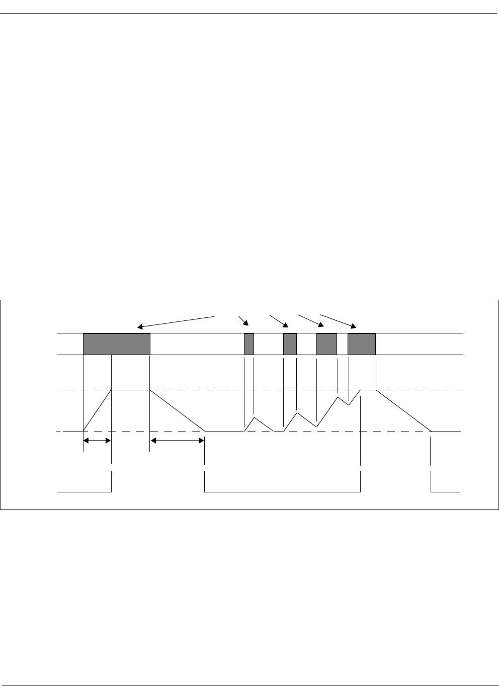
Guard Soak Timer (GST)
The GST block mimics the operation of an analog integrator by accumulating failure events from the CFM and the
SCM blocks and applying a selectable rate of decay when no failures are detected.
As shown in Figure 5, a GST failure (gst_fail) is triggered when the accumulated failures have reached the upper
threshold during the disqualification observation window. When there are no CFM or SCM failures, the accumulator
decrements until it reaches its lower threshold during the qualification window.
Figure 5 - Behaviour of the Guard Soak Timer during CFM or SCM Failures
All sync inputs (sync0 to sync2) are continuously monitored to ensure that there is a correct number of reference
clock cycles within the frame pulse period.
1.5 Output Clocks and Frame Pulses
The ZL30123 offers a wide variety of outputs including two low-jitter differential LVPECL clocks (diff0_p/n,
diff1_p/n), two SONET/SDH LVCMOS (sdh_clk0, sdh_clk1) output clocks and four programmable LVCMOS
(p0_clk0, p0_clk1, p1_clk0, p1_clk1) output clocks. In addition to the clock outputs, two LVCMOS SONET/SDH
frame pulse outputs (sdh_fp0, sdh_fp1) and two LVCMOS programmable frame pulses (p0_fp0, p0_fp1) are also
available.
ref
CFM or SCM failures
upper threshold
lower threshold
t
d
- disqualification time
t
q
- qualification time = n * t
d
t
d
t
q
gst_fail

ZL30123GGG2

Mfr. #:
Manufacturer:
Microchip / Microsemi
Description:
Clock Generators & Support Products Pb Free SONET/SDH PLL Line Card Synch.
Lifecycle:
New from this manufacturer.
Delivery:
DHL FedEx Ups TNT EMS
Payment:
T/T Paypal Visa MoneyGram Western Union

Products related to this Datasheet