10 DS734F5
5.4 Power Supply Characteristics
5.4 Power Supply Characteristics
(Measurements performed under operating conditions)
5.5 Thermal Data (48-pin LQFP)
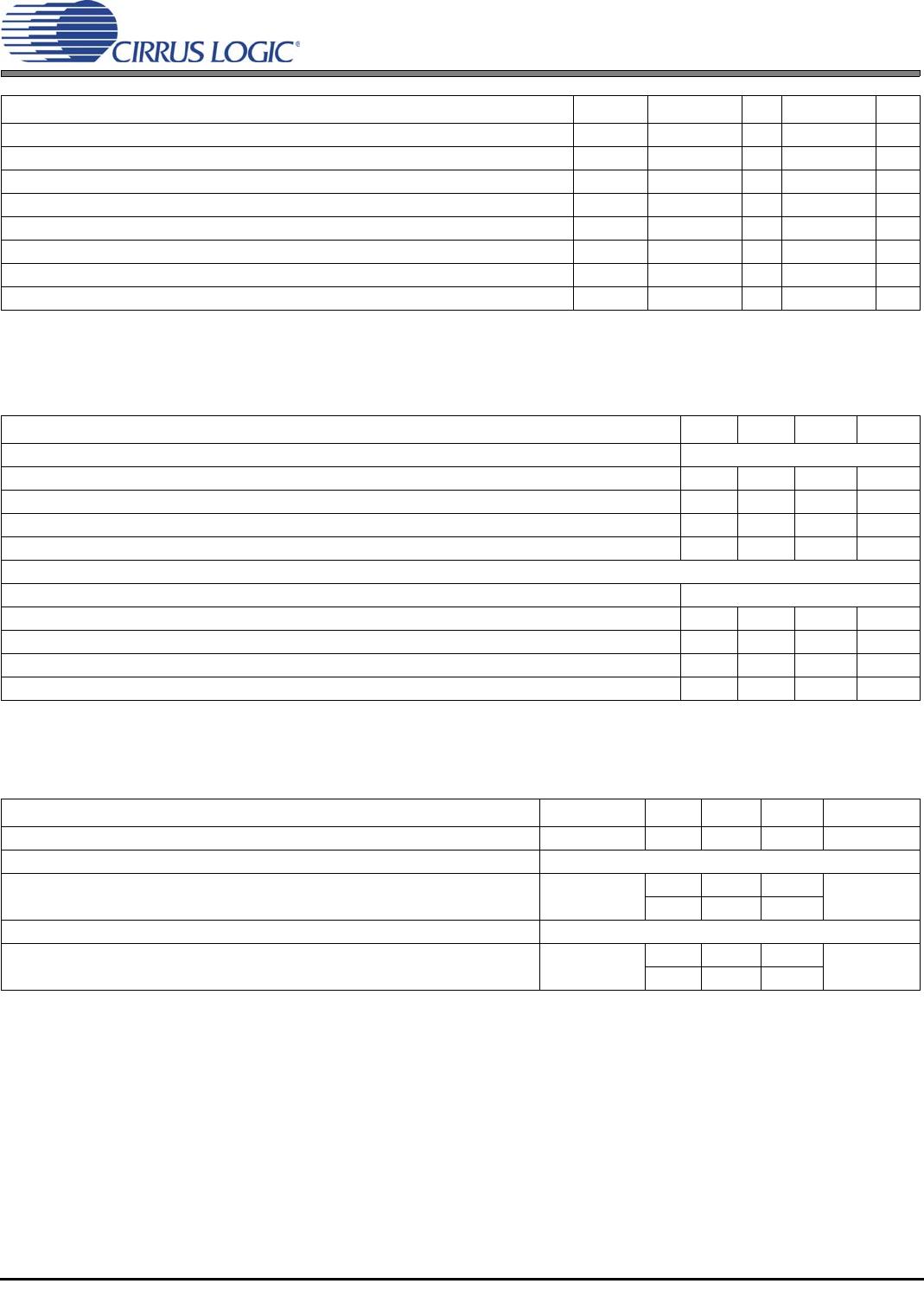
Parameter Symbol Min Typ Max Unit
High-level input voltage V
IH
2.0 — — V
Low-level input voltage, except XTI V
IL
——0.8V
Low-level input voltage, XTI V
ILXTI
——0.6V
Input hysteresis V
hys
—0.4— V
High-level output voltage (I
O
= –2 mA), except XTI V
OH
VDDIO*0.9 — — V
Low-level output voltage (I
O
= 2 mA), except XTI V
OL
——VDDIO*0.1V
Input leakage XTI I
LXTI
—— 5 µA
Input leakage current (all digital pins with internal pull-up resistors enabled) I
LEAK
——70µA
Parameter Min Typ Max Unit
Operational Power Supply Current:
VDD: Core and I/O operating
1
1.Dependent on application firmware and DSP clock speed.
— 203 — mA
VDDA: PLL operating —8 —mA
VDDIO: With most ports operating —27 — mA
Total Operational Power Dissipation: — 480 — mW
Standby Power Supply Current:
VDD: Core and I/O not clocked — 100 — µA
VDDA: PLL halted —1 —µA
VDDIO: All connected I/O pins 3-stated by other ICs in system — 50 — µA
Total Standby Power Dissipation — 348 — µW
Parameter Symbol Min Typ Max Unit
Junction Temperature T
j
——125 °C
Thermal Resistance (Junction to Ambient)
Two-layer board
1
Four-layer board
2
1.Two-layer board is specified as a 76 mm X 114 mm, 1.6 mm thick FR-4 material with 1 oz. copper covering 20% of the top and bottom layers.
2.Four-layer board is specified as a 76 mm X 114 mm, 1.6 mm thick FR-4 material with 1 oz. copper covering 20% of the top and bottom layers and 0.5
oz. copper covering 90 % of the internal power plane and ground plane layers.
θ
ja
— 63.5 — °C/Watt
—54 —
Thermal Resistance (Junction to Top of Package)
Two-layer board
3
Four-layer board
4
3.To calculate the die temperature for a given power dissipation
T
j
= Ambient Temperature + [(Power Dissipation in Watts)*θ
ja
]
4.To calculate the case temperature for a given power dissipation
T
c
= T
j
– [(Power Dissipation in Watts)*ψ
jt
]
ψ
jt
— 0.70 — °C/Watt
—0.64 —

