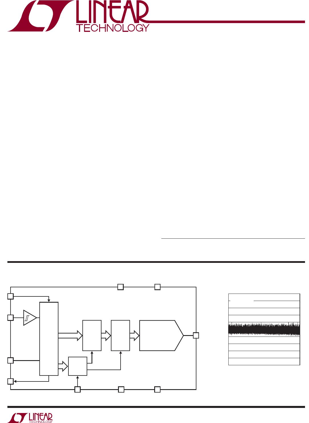
LTC2601/LTC2611/LTC2621
2
2601fb
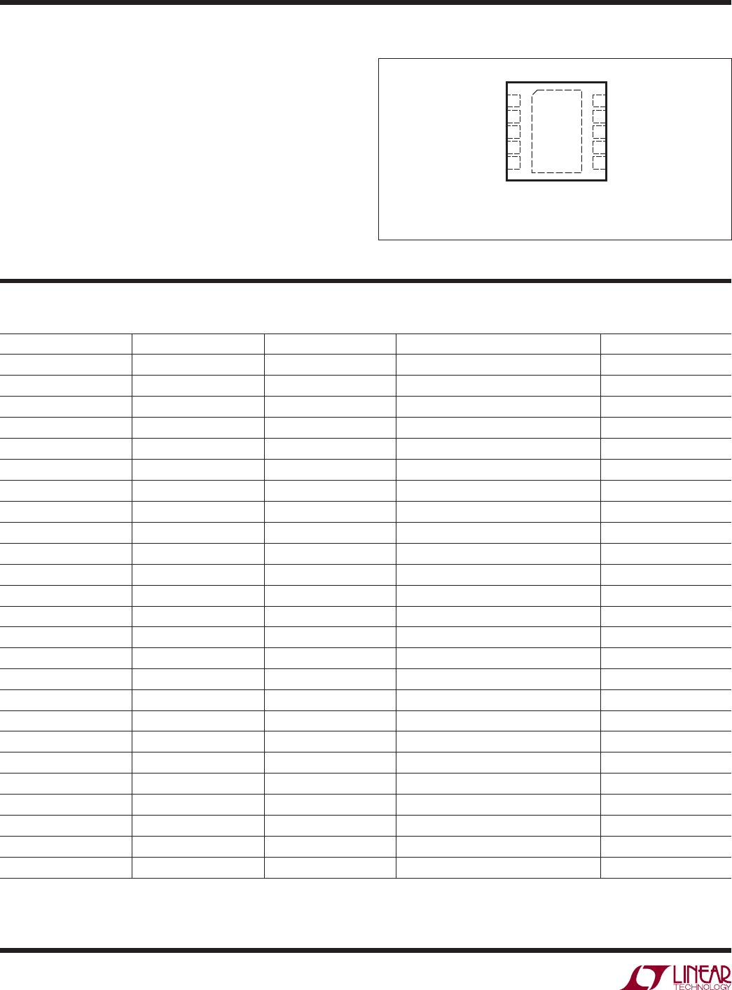
PIN CONFIGURATION ABSOLUTE MAXIMUM RATINGS
Any Pin to GND ............................................ –0.3V to 6V
Any Pin to V
CC
.............................................. –6V to 0.3V
Maximum Junction Temperature........................... 125°C
Storage Temperature Range ...................–65°C to 125°C
Lead Temperature (Soldering, 10 sec) .................. 300°C
Operating Temperature Range:
LTC2601C/LTC2611C/LTC2621C
LTC2601C-1/LTC2611C-1/LTC2621C-1 .... 0°C to 70°C
LTC2601I/LTC2611I/LTC2621I
LTC2601I-1/LTC2611I-1/LTC2621I-1 ....–40°C to 85°C
(Note 1)
TOP VIEW
11
DD PACKAGE
10-LEAD (3mm s 3mm) PLASTIC DFN
10
9
6
7
8
4
5
3
2
1
LDA
V
CC
GND
V
OUT
REF
SDO
SDI
SCK
CLR
CS/LD
T
JMAX
= 125°C, θ
JA
= 43°C/W
EXPOSED PAD (PIN 11) IS GND, MUST BE SOLDERED TO PCB
ORDER INFORMATION
LEAD FREE FINISH TAPE AND REEL PART MARKING* PACKAGE DESCRIPTION TEMPERATURE RANGE
LTC2601CDD#PBF LTC2601CDD#TRPBF LAGT
10-Lead (3mm × 3mm) Plastic DFN
0°C to 70°C
LTC2601IDD#PBF LTC2601IDD#TRPBF LAGT
10-Lead (3mm × 3mm) Plastic DFN
–40°C to 85°C
LTC2611CDD#PBF LTC2611CDD#TRPBF LBFQ
10-Lead (3mm × 3mm) Plastic DFN
0°C to 70°C
LTC2611IDD#PBF LTC2611IDD#TRPBF LBFQ
10-Lead (3mm × 3mm) Plastic DFN
–40°C to 85°C
LTC2621CDD#PBF LTC2621CDD#TRPBF LBFS
10-Lead (3mm × 3mm) Plastic DFN
0°C to 70°C
LTC2621IDD#PBF LTC2621IDD#TRPBF LBFS
10-Lead (3mm × 3mm) Plastic DFN
–40°C to 85°C
LTC2601CDD-1#PBF LTC2601CDD-1#TRPBF LBZH
10-Lead (3mm × 3mm) Plastic DFN
0°C to 70°C
LTC2601IDD-1#PBF LTC2601IDD-1#TRPBF LBZH
10-Lead (3mm × 3mm) Plastic DFN
–40°C to 85°C
LTC2611CDD-1#PBF LTC2611CDD-1#TRPBF LBZJ
10-Lead (3mm × 3mm) Plastic DFN
0°C to 70°C
LTC2611IDD-1#PBF LTC2611IDD-1#TRPBF LBZJ
10-Lead (3mm × 3mm) Plastic DFN
–40°C to 85°C
LTC2621CDD-1#PBF LTC2621CDD-1#TRPBF LBZK
10-Lead (3mm × 3mm) Plastic DFN
0°C to 70°C
LTC2621IDD-1#PBF LTC2621IDD-1#TRPBF LBZK
10-Lead (3mm × 3mm) Plastic DFN
–40°C to 85°C
LEAD BASED FINISH TAPE AND REEL PART MARKING* PACKAGE DESCRIPTION TEMPERATURE RANGE
LTC2601CDD LTC2601CDD#TR LAGT
10-Lead (3mm × 3mm) Plastic DFN
0°C to 70°C
LTC2601IDD LTC2601IDD#TR LAGT
10-Lead (3mm × 3mm) Plastic DFN
–40°C to 85°C
LTC2611CDD LTC2611CDD#TR LBFQ
10-Lead (3mm × 3mm) Plastic DFN
0°C to 70°C
LTC2611IDD LTC2611IDD#TR LBFQ
10-Lead (3mm × 3mm) Plastic DFN
–40°C to 85°C
LTC2621CDD LTC2621CDD#TR LBFS
10-Lead (3mm × 3mm) Plastic DFN
0°C to 70°C
LTC2621IDD LTC2621IDD#TR LBFS
10-Lead (3mm × 3mm) Plastic DFN
–40°C to 85°C
LTC2601CDD-1 LTC2601CDD-1#TR LBZH
10-Lead (3mm × 3mm) Plastic DFN
0°C to 70°C
LTC2601IDD-1 LTC2601IDD-1#TR LBZH
10-Lead (3mm × 3mm) Plastic DFN
–40°C to 85°C
LTC2611CDD-1 LTC2611CDD-1#TR LBZJ
10-Lead (3mm × 3mm) Plastic DFN
0°C to 70°C
LTC2611IDD-1 LTC2611IDD-1#TR LBZJ
10-Lead (3mm × 3mm) Plastic DFN
–40°C to 85°C
LTC2621CDD-1 LTC2621CDD-1#TR LBZK
10-Lead (3mm × 3mm) Plastic DFN
0°C to 70°C
LTC2621IDD-1 LTC2621IDD-1#TR LBZK
10-Lead (3mm × 3mm) Plastic DFN
–40°C to 85°C
Consult LTC Marketing for parts specifi ed with wider operating temperature ranges. *The temperature grade is identifi ed by a label on the shipping container.
For more information on lead free part marking, go to:
http://www.linear.com/leadfree/
For more information on tape and reel specifi cations, go to:
http://www.linear.com/tapeandreel/