74LVC16244APAG

INDUSTRIAL TEMPERATURE RANGE
IDT74LVC16244A
3.3V CMOS 16-BIT BUFFER/DRIVER WITH 3-STATE OUTPUTS
1
JULY 2015INDUSTRIAL TEMPERATURE RANGE
IDT and the IDT logo is a registered trademark of Integrated Device Technology, Inc.
© 2015 Integrated Device Technology, Inc. DSC-4726/6
FEATURES:
Typical tSK(o) (Output Skew) < 250ps
ESD > 2000V per MIL-STD-883, Method 3015; > 200V using
machine model (C = 200pF, R = 0)
•VCC = 3.3V ± 0.3V, Normal Range
•VCC = 2.7V to 3.6V, Extended Range
CMOS power levels (0.4
μμ
μμ
μ W typ. static)
All inputs, outputs, and I/O are 5V tolerant
Supports hot insertion
Available in SSOP and TSSOP packages
FUNCTIONAL BLOCK DIAGRAM
APPLICATIONS:
5V and 3.3V mixed voltage systems
Data communication and telecommunication systems
DRIVE FEATURES:
High Output Drivers: ±24mA
Reduced system switching noise
3.3V CMOS 16-BIT
BUFFER/DRIVER
WITH 3-STATE OUTPUTS,
5 VOLT TOLERANT I/O
IDT74LVC16244A
DESCRIPTION:
The LVC16244A 16-bit buffer/driver is built using advanced dual metal
CMOS technology. The LVC16244A is designed specifically to improve
both the performance and density of 3-state memory address drivers, clock
drivers, and bus-oriented receivers and transmitters. The device can be
used as four 4-bit buffers, two 8-bit buffers, or one 16-bit buffer. This device
provides true outputs and symmetrical active-low output-enable (OE)
inputs.
All pins of this 16-bit buffer/driver can be driven from either 3.3V or 5V
devices. This feature allows the use of the device as a translator in a mixed
3.3V/5V supply system.
The LVC16244A has been designed with a ±24mA output driver. This
driver is capable of driving a moderate to heavy load while maintaining
speed performance.
1A1
1
A2
1
A3
1
A4
1
Y1
1
OE
1Y2
1
Y3
1
Y4
2A1
2
A2
2
A3
2
A4
2
Y1
2
OE
2Y2
2
Y3
2
Y4
3A1
3
A2
3
A3
3
A4
3
Y1
3
OE
3Y2
3
Y3
3
Y4
4A1
4
A2
4
A3
4
A4
4
Y1
4
OE
4Y2
4
Y3
4
Y4
1
47
46
44
43
48
41
40
38
37
25
36
35
33
32
24
30
29
27
26
13
14
16
17
19
20
22
23
2
3
5
6
8
9
11
12
INDUSTRIAL TEMPERATURE RANGE
2
IDT74LVC16244A
3.3V CMOS 16-BIT BUFFER/DRIVER WITH 3-STATE OUTPUTS
SSOP / TSSOP
TOP VIEW
PIN CONFIGURATION
NOTES:
1. H = HIGH Voltage Level
X = Don’t Care
L = LOW Voltage Level
Z = High-Impedance
Inputs Outputs
xOE xAx xYx
LLL
LHH
HXZ
FUNCTION TABLE (EACH 4-BIT BUFFER)
(1)
Pin Names Description
x A x Data Inputs
x Y x 3-State Outputs
xOE 3-State Output Enable Inputs (Active LOW)
PIN DESCRIPTION
NOTE:
1. As applicable to the device type.
Symbol Parameter
(1)
Conditions Typ. Max. Unit
CIN Input Capacitance VIN = 0V 4.5 6 pF
COUT Output Capacitance VOUT = 0V 6.5 8 pF
C
I/O I/O Port Capacitance VIN = 0V 6.5 8 pF
CAPACITANCE (TA = +25°C, F = 1.0MHz)
Symbol Description Max Unit
VTERM
(2)
Terminal Voltage with Respect to GND –0.5 to +6.5 V
VTERM
(3)
Terminal Voltage with Respect to GND –0.5 to +6.5 V
TSTG Storage Temperature –65 to +150 °C
IOUT DC Output Current –50 to +50 mA
I
IK Continuous Clamp Current, 50 mA
IOK VI < 0 or VO < 0
I
CC Continuous Current through each ±100 mA
ISS VCC or GND
ABSOLUTE MAXIMUM RATINGS
(1)
NOTES:
1. Stresses greater than those listed under ABSOLUTE MAXIMUM RATINGS may cause
permanent damage to the device. This is a stress rating only and functional operation
of the device at these or any other conditions above those indicated in the operational
sections of this specification is not implied. Exposure to absolute maximum rating
conditions for extended periods may affect reliability.
2. VCC terminals.
3. All terminals except VCC.
1OE
1Y1
1
Y2
GND
1Y3
1
Y4
VCC
2
Y1
2
Y2
GND
2Y3
2
Y4
3
Y1
3
Y2
3
Y4
4
OE
GND
V
CC
4
Y1
4
Y2
GND
4Y3
2
3
4
5
6
7
8
9
10
11
12
13
14
15
16
17
18
19
20
21
22
23
24
39
38
37
36
35
34
33
32
31
30
29
28
27
26
25
40
41
42
43
44
45
46
47
481
2OE
1A1
1
A2
GND
1A3
1
A4
VCC
2
A1
2
A2
2
A3
2
A4
3
A1
GND
3A3
3
A4
4
A1
4
A2
GND
4A3
4
A4
3
OE
3Y3
4
Y4
VCC
3
A2
GND
INDUSTRIAL TEMPERATURE RANGE
IDT74LVC16244A
3.3V CMOS 16-BIT BUFFER/DRIVER WITH 3-STATE OUTPUTS
3
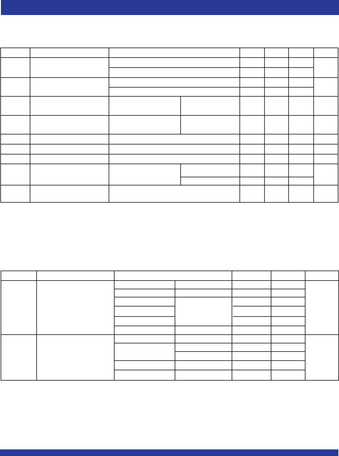
Symbol Parameter Test Conditions Min. Typ.
(1)
Max. Unit
VIH Input HIGH Voltage Level VCC = 2.3V to 2.7V 1.7 V
VCC = 2.7V to 3.6V 2
V
IL Input LOW Voltage Level VCC = 2.3V to 2.7V 0.7 V
VCC = 2.7V to 3.6V 0.8
I
IH Input Leakage Current VCC = 3.6V VI = 0 to 5.5V ±5 μA
IIL
IOZH High Impedance Output Current VCC = 3.6V VO = 0 to 5.5V ±10 μA
IOZL (3-State Output pins)
IOFF Input/Output Power Off Leakage VCC = 0V, VIN or VO 5.5V ±50 μA
VIK Clamp Diode Voltage VCC = 2.3V, IIN = –18mA –0.7 –1.2 V
VH Input Hysteresis VCC = 3.3V 100 mV
I
CCL Quiescent Power Supply Current VCC = 3.6V VIN = GND or VCC —— 10μA
ICCH
ICCZ 3.6 VIN 5.5V
(2)
—— 10
ΔICC Quiescent Power Supply Current One input at VCC - 0.6V, other inputs at VCC or GND 500 μA
Variation
DC ELECTRICAL CHARACTERISTICS OVER OPERATING RANGE
Following Conditions Apply Unless Otherwise Specified:
Operating Condition: TA = –40°C to +85°C
NOTES:
1. Typical values are at VCC = 3.3V, +25°C ambient.
2. This applies in the disabled state only.
NOTE:
1. VIH and VIL must be within the min. or max. range shown in the DC ELECTRICAL CHARACTERISTICS OVER OPERATING RANGE table for the appropriate VCC range.
TA = – 40°C to + 85°C.
OUTPUT DRIVE CHARACTERISTICS
Symbol Parameter Test Conditions
(1)
Min. Max. Unit
VOH Output HIGH Voltage VCC = 2.3V to 3.6V IOH = – 0.1mA VCC – 0.2 V
VCC = 2.3V IOH = – 6mA 2
VCC = 2.3V IOH = – 12mA 1.7
VCC = 2.7V 2.2
VCC = 3V 2.4
VCC = 3V IOH = – 24mA 2.2
VOL Output LOW Voltage VCC = 2.3V to 3.6V IOL = 0.1mA 0.2 V
VCC = 2.3V IOL = 6mA 0.4
IOL = 12mA 0.7
VCC = 2.7V IOL = 12mA 0.4
VCC = 3V IOL = 24mA 0.55

74LVC16244APAG

Mfr. #:
Manufacturer:
IDT
Description:
Buffers & Line Drivers 16-bit Buffer/Driver w/3-State Outputs
Lifecycle:
New from this manufacturer.
Delivery:
DHL FedEx Ups TNT EMS
Payment:
T/T Paypal Visa MoneyGram Western Union