INDUSTRIAL TEMPERATURE RANGE
4
IDT74LVC16244A
3.3V CMOS 16-BIT BUFFER/DRIVER WITH 3-STATE OUTPUTS
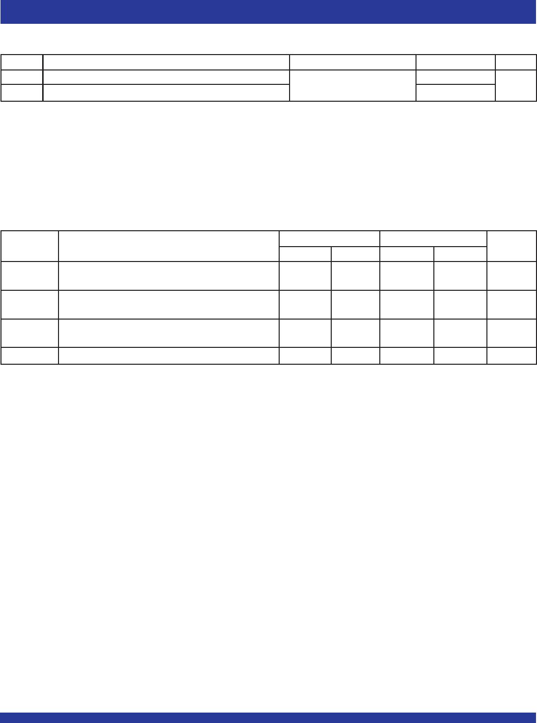
OPERATING CHARACTERISTICS, VCC = 3.3V ± 0.3V, TA = 25°C
Symbol Parameter Test Conditions Typical Unit
CPD Power Dissipation Capacitance per Buffer/Driver Outputs enabled CL = 0pF, f = 10Mhz 34 pF
CPD Power Dissipation Capacitance per Buffer/Driver Outputs disabled 3
SWITCHING CHARACTERISTICS
(1)
VCC = 2.7V VCC = 3.3V ± 0.3V
Symbol Parameter Min. Max. Min. Max. Unit
tPLH Propagation Delay — 4.7 1.1 4.1 ns
tPHL xAx to xYx
tPZH Output Enable Time — 5.8 1 4.6 ns
tPZL xOE to xYx
tPHZ Output Disable Time — 6.2 1.8 5.8 ns
tPLZ xOE to xYx
t
SK(o) Output Skew
(2)
—— — 1ns
NOTES:
1. See TEST CIRCUITS AND WAVEFORMS. TA = – 40°C to + 85°C.
2. Skew between any two outputs of the same package and switching in the same direction.