PEDR45V032A-05
MR45V032A
16/20
Timing Diagrams
Serial Input Timing
Hold Timing
Output Timing
CS
#
t
CHSL
SC
K
SI
SO
MSB IN LSB IN
High Impedance
t
SLCH
t
DVCH
t
CHDX
t
CLCH
t
CHCL
t
SHCH
t
CHSH
t
SHSL
CS
#
SC
K
SO
SI
HOLD
#
t
CHHL
t
HLCH
t
HHCH
t
HHQX
t
CHHH
t
HLQ
Z
CS
#
SC
K
SO
SI
A
ddress, LSB IN
t
CH
t
CL
t
SHQ
Z
t
CLQV
t
CLQX
t
CLQX
t
CLQV
t
QLQH
t
QHQL
LSB OUT
PEDR45V032A-05
MR45V032A
17/20
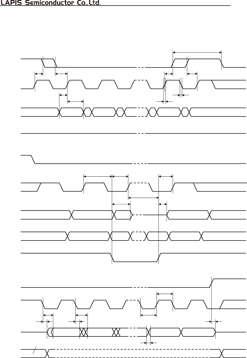
Power-On and Power-Off Characteristics
(Under recommended operating conditions)
Parameter Symbol Min. Max. Unit Note
Power-On CS# High Hold Time
t
VHEL
20 s 1, 2
Power-Off CS# High Hold Time
t
EHVL
100 ns 1
Power-On Interval Time
t
VLVH
1 s 2
Power-On time
tR 50  s/V
Power-Off time
tF 100  s/V
Notes:
1. To prevent an erroneous operation, be sure to maintain CS#="H", and set the FeRAM in an inactive state
(standby mode) before and after power-on and power-off.
2. Powering on at the intermediate voltage level will cause an erroneous operation; thus, be sure to power up
from 0 V.
3. Enter all signals at the same time as power-on or enter all signals after power-on.
Power-On and Power-Off Sequences
0
V
V
IL
Max.
V
CC
Min.
V
CC
V
IH
Min.
CS#
0V
V
IL
Max.
V
CC
Min.
V
CC
V
IH
Min.
CS#
t
VHEL
t
VLVH
t
EHVL
t
R
t
F
PEDR45V032A-05
MR45V032A
18/20
Read/Write Cycles and Data Retention
(Under recommended operating conditions)
Parameter Min. Max. Unit Note
Read/Write Cycle
10
12
Cycle
Data Retention
10 Year
Capacitance
Signal Symbol Min. Max. Unit Note
Input Capacitance
C
IN
10 pF 1
Input/Output Capacitance
C
OUT
10 pF 1
Note:
Sampling value. Measurement conditions are V
IN
= V
OUT
= GND, f = 1MHz, and Ta = 25°C

MR45V032AMAZBATL

Mfr. #:
Manufacturer:
Description:
F-RAM 32K; SPI; 3.3V FeRAM 15MHz
Lifecycle:
New from this manufacturer.
Delivery:
DHL FedEx Ups TNT EMS
Payment:
T/T Paypal Visa MoneyGram Western Union

Products related to this Datasheet