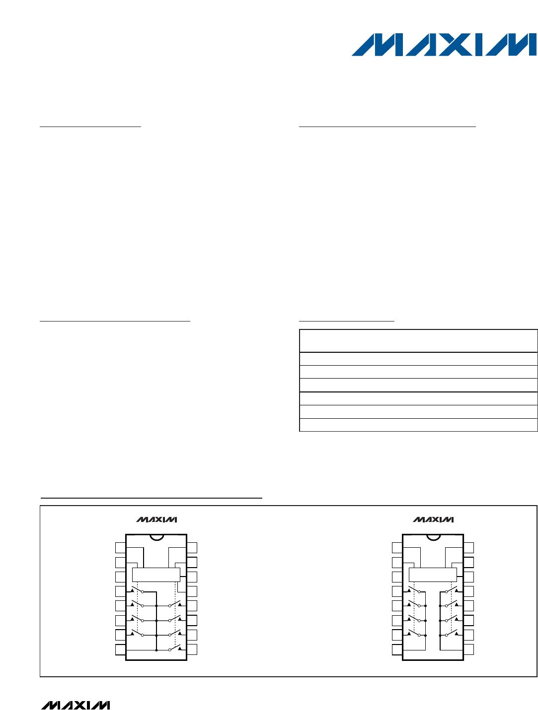
General Description
The MAX4508/MAX4509 are 8-to-1 and dual 4-to-1 fault-
protected multiplexers that are pin compatible with the
industry-standard DG508/DG509. The MAX4508/
MAX4509 operate with dual supplies of ±4.5V to ±20V or
a single supply of +9V to +36V. These multiplexers fea-
ture fault-protected inputs, rail-to-rail signal handling
capability, and overvoltage clamping at 150mV beyond
the rails.
Both parts offer ±40V overvoltage protection with sup-
plies off and ±25V protection with supplies on. On-
resistance is 400Ω max and is matched between
channels to 15Ω max. All digital inputs have TTL logic
thresholds, ensuring both TTL and CMOS logic com-
patibility when using a single +12V supply or dual ±15V
supplies.
Applications
Data-Acquisition Systems
Industrial and Process Control
Avionics
Signal Routing
Redundant/Backup Systems
Features
±40V Fault Protection with Power Off
±25V Fault Protection with ±15V Supplies
Rail-to-Rail Signal Handling
No Power-Supply Sequencing Required
All Channels Off with Power Off
Output Clamped to Appropriate Supply Voltage
During Fault Condition
1kΩ Output Clamp Resistance During
Overvoltage
400
ΩΩ
max On-Resistance
20ns Fault-Response Time
±4.5V to ±20V Dual Supplies
+9V to +36V Single Supply
TTL/CMOS-Compatible Logic Inputs
MAX4508/MAX4509
Fault-Protected, High-Voltage Single 8-to-1/
Dual 4-to-1 Multiplexers with Output Clamps
________________________________________________________________ Maxim Integrated Products 1
16
15
14
13
12
11
10
9
1
2
3
4
5
6
7
8
A1
A2
GND
V+
NO1
V-
EN
A0
TOP VIEW
MAX4508
NO5
NO6
NO7
NO8
COM
NO4
NO3
NO2
SO/DIP
LOGIC
16
15
14
13
12
11
10
9
1
2
3
4
5
6
7
8
A1
GND
V+
NO1B
NO1A
V-
EN
A0
MAX4509
NO2B
NO3B
NO4B
COMB
COMA
NO4A
NO3A
NO2A
SO/DIP
LOGIC
Pin Configurations/Functional Diagrams
19-1414; Rev 5; 10/07
Ordering Information continued at end of data sheet.
*Contact factory for dice specifications.
**Contact factory for availability.
+Denotes a lead-free package.
Functional Diagrams/Truth Tables appear at end of
data sheet.
Ordering Information
For pricing, delivery, and ordering information, please contact Maxim Direct at 1-888-629-4642,
or visit Maxim’s website at www.maxim-ic.com.
PART
TEMP
RANGE
PIN-
PACKAGE
PKG
CODE
MAX4508CSE+
0°C to +70°C 16 Narrow SO
S16-8
MAX4508CPE+
0°C to +70°C 16 Plastic DIP
P16-4
MAX4508C/D
0°C to +70°C
Dice*
MAX4508ESE+
-40°C to +85°C 16 Narrow SO
S16-8
MAX4508EPE+
-40°C to +85°C 16 Plastic DIP
P16-4
MAX4508MJE
-40°C to +85°C
16 CERDIP** J16-3
MAX4508/MAX4509
Fault-Protected, High-Voltage Single 8-to-1/
Dual 4-to-1 Multiplexers with Output Clamps
2 _______________________________________________________________________________________
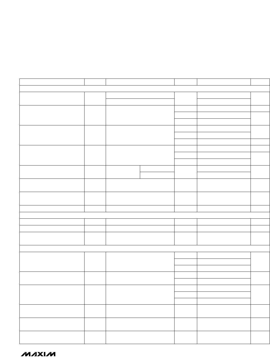
ABSOLUTE MAXIMUM RATINGS
ELECTRICAL CHARACTERISTICS—Dual Supplies
(V+ = +15V, V- = -15V, V
A_
H
=+2.4V, V
A_
L
= +0.8V, V
EN
= +2.4V, T
A
= T
MIN
to T
MAX
, unless otherwise noted. Typical values are at
T
A
= +25°C.) (Note 2)
Stresses beyond those listed under “Absolute Maximum Ratings” may cause permanent damage to the device. These are stress ratings only, and functional
operation of the device at these or any other conditions beyond those indicated in the operational sections of the specifications is not implied. Exposure to
absolute maximum rating conditions for extended periods may affect device reliability.
(Voltages Referenced to GND)
V+ ........................................................................-0.3V to +44.0V
V- .........................................................................-44.0V to +0.3V
V+ to V-................................................................-0.3V to +44.0V
COM_, A_ (Note 1) .............................. (V+ + 0.3V) to (V- - 0.3V)
NO_.........................................................(V+ - 40V) to (V- + 40V)
NO_ to COM_ ..........................................................-36V to +36V
NO_ Overvoltage with Switch Power On. ................-30V to +30V
NO_ Overvoltage with Switch Power Off. ................-40V to +40V
Continuous Current into Any Terminal..............................±30mA
Peak Current, into Any Terminal
(pulsed at 1ms, 10% duty cycle).................................±100mA
Continuous Power Dissipation (T
A
= +70°C)
16 Narrow SO (derate 8.70mW/°C above +70°C) ........696mW
16-Pin PDIP (derate 10.53mW/°C above +70°C)..........842mW
16-Pin CERDIP (derate 10.00mW/°C above +70°C).....800mW
Operating Temperature Ranges
MAX4508C_ E/MAX4509C_E...............................0°C to +70°C
MAX4508E_ E/MAX4509E_E ............................-40°C to +85°C
MAX4508MJE/MAX4509MJE..........................-55°C to +125°C
Storage Temperature Range .............................-65°C to +160°C
Lead Temperature (soldering, 10s) .................................+300°C
Note 1: COM_, EN, and A_ pins are not fault protected. Signals on COM_, EN, or A_ exceeding V+ or V- are clamped by internal
diodes. Limit forward diode current to maximum current rating.
-150 +150
-15 +75
-1 +1
COM_ On-Leakage Current
(Note 6)
-300 +300
-100 +75
nA
-2 +2
I
COM_(ON)
-100 +100
COM_ Off-Leakage Current
(Note 6)
-100 +75
-1 +1
-200 +200
-20 +75
nA
-2 +2
I
COM_(OFF)
300 400
R
ON
V
V- V+
V
NO_
Fault-Free Analog Signal Range
(Notes 3, 4)
-50 +50
I
NO_(OFF)
NO_ Off-Leakage Current
(Note 6)
-5 +5
nA
-0.5 +0.5
25
500
Ω
700
On-Resistance
Ω
15
ΔR
ON
On-Resistance Match Between
Channels (Note 5)
20
UNITSMIN TYP MAXSYMBOLPARAMETER
V+ = +15V, V- = -15V,
V
NO_
= ±15V
V
COM_
= ±10V,
V
NO_
= ±10V or
floating
V
NO_
= ±10V, V
COM_
=
+10V
V
COM_
= ±10V, I
NO_
= 0.2mA
V
COM_
= ±10V, I
NO_
= 0.2mA
V
COM_
= ±10V,
V
NO_
=
+10V
CONDITIONS
M
C, E
+25°C
+25°C
M
C, E, M
C, E
+25°C
M
C, E
M
C, E
+25°C
M
+25°C
M
C, E
M
+25°C
C, E
C, E
+25°C
T
A
MAX4508
MAX4509
MAX4508
MAX4509
ANALOG SWITCH
MAX4508/MAX4509
Fault-Protected, High-Voltage Single 8-to-1/
Dual 4-to-1 Multiplexers with Output Clamps
_______________________________________________________________________________________ 3
ELECTRICAL CHARACTERISTICS—Dual Supplies (continued)
(V+ = +15V, V- = -15V, V
A_
H
= +2.4V, V
A_
L
= +0.8V, V
EN
= +2.4V, T
A
= T
MIN
to T
MAX
, unless otherwise noted. Typical values are at
T
A
= +25°C.) (Note 2)
V
NO_
= ±25VR
COM_
ns
600
ns
Enable Turn-On Time
120 200
M
Transition Time
+25°C
500
170 350
t
TRANS
Figure 2
C, E, M
+25°C
V
NO_
= ±10V, R
L
= 1kΩ,
Figures 2 and 3
nst
OFF
Enable Turn-Off Time 250C, E
10 80C, E, M
V
NO_
= ±10V, R
L
= 1kΩ,
Figure 4
ns
400M
t
BBM
Break-Before-Make Time Delay
(Note 4)
UNITSMIN TYP MAXSYMBOLPARAMETER CONDITIONS TA
400
160 275
t
ON
µA-1 +1I
A_H
, I
A_L
A_ Input Current Logic
High or Low
V0.8V
A_L
A_ Input Logic Threshold Low
V2.4V
A_H
A_ Input Logic Threshold High
µs2.5± Fault Recovery Time (Note 4)
ns20
± Fault Output Clamp Turn-On
Delay (Note 4)
COM_ On Clamp Output
Resistance, Supplies On
kΩ100 1.0 2.5
COM_ On Clamp Output
Current, Supplies On
-13 -11 -7
mA
71013
I
COM_
nA-20 +20
-40 +40
V
-25 +25
V
NO_
Fault-Protected Analog Signal
Range (Notes 3, 4)
µA
-100 +100
nA
-5 +5
-20 +20
I
NO_
NO_ Input Leakage Current,
Supplies Off
µA-50 +50
I
NO_
NO_ Input Leakage Current,
Supplies On
-1 +1
-100 +100
I
COM_
COM_ Output Leakage Current,
Supplies On
nA
-20 +20
-200 +200
V
NO_
= ±10V, R
L
= 1kΩ,
Figures 2 and 3
V
A_
= 0.8V or 2.4V
Applies with power on, Figure 9
R
L
= 10kΩ, V
NO_
= ±25V
R
L
= 10kΩ, V
NO_
= ±25V
V
NO_
= ±40V, V
COM
= 0,
V+ = 0, V- = 0
V
NO_
= ±25V, V
COM_
=
+10V,
V
EN
= 0
V
NO_
= ±25V, V
EN
= 0
V
COM
= 0
C, E
+25°C
+25°C
C, E, M
C, E, M
C, E, M
+25°C
+25°C
+25°C
M
C, E
+25°C
+25°C
M
C, E
M
+25°C
C, E
+25°C
210+25°C
C
L
= 1.0nF, V
NO_
= 0, R
S
= 0,
Figure 5
pCQCharge Injection (Note 4)
-70+25°C
R
L
= 75Ω, C
L
= 15pF,
V
NO_
= 1V
RMS
, f = 1MHz, Figure 6
dBV
ISO
Off-Isolation (Note 7)
SWITCH DYNAMIC CHARACTERISTICS
LOGIC INPUT
FAULT PROTECTION
Applies with power off
V
NO_
= +25V
V
NO_
= -25V
µA

MAX4508EPE+

Mfr. #:
Manufacturer:
Maxim Integrated
Description:
Multiplexer Switch ICs 8:1 Fault Protected Analog MUX
Lifecycle:
New from this manufacturer.
Delivery:
DHL FedEx Ups TNT EMS
Payment:
T/T Paypal Visa MoneyGram Western Union