MAX4508/MAX4509
Fault-Protected, High-Voltage Single 8-to-1/
Dual 4-to-1 Multiplexers with Output Clamps
______________________________________________________________________________________ 11
combination of N1 and P1 forms a low-value resistor
between NO_ and COM_ so that signals pass equally
well in either direction.
Positive Fault Condition
When the signal on NO_ exceeds V+ by about 150mV,
the positive fault comparator output goes high, turning
off FETs N1 and P1 (Figure 1). This makes the NO_ pin
high impedance, regardless of the switch state. If the
switch state is “off,” all FETs turn off, and both NO_ and
COM_ are high impedance. If the switch state is “on,”
FET P2 turns on, clamping COM_ to V+.
Negative Fault Condition
When the signal on NO_ goes about 150mV below V-,
the negative fault comparator output goes high, turning
off FETs N1 and P1 (Figure 1). This makes the NO_ pin
high impedance, regardless of the switch state. If the
switch state is “off,” all FETs turn off, and both NO_ and
COM_ are high impedance. If the switch state is “on,”
FET N2 turns on, clamping COM_ to V-.
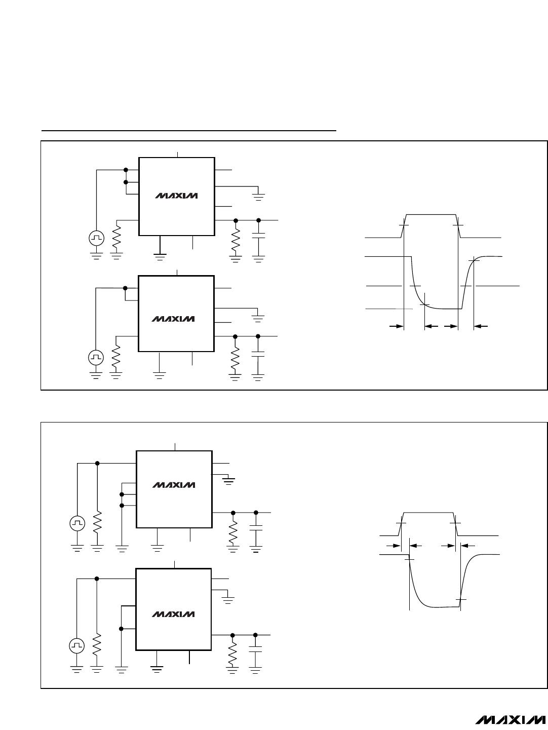
Transient Fault Condition
When a fast rising or falling transient on NO_ exceeds
V+ or V-, the output (COM_) follows the input (NO_) to
the supply rail with only a few nanoseconds delay. This
delay is due to the switch on-resistance and circuit
capacitance to ground. When the input transient
returns to within the supply rails, however, there is a
longer output recovery time. For positive faults, the
recovery time is typically 2.5µs (see Typical Operating
Characteristics). For negative faults, the recovery time
is typically 1.3µs. These values depend on the COM_
output resistance and capacitance. The delays do not
depend on the fault amplitude. Higher COM_ output
resistance and capacitance increase the recovery
times.
COM and A_
FETs N2 and P2 can source about ±10mA from V+ or
V- to the COM_ pin in the fault condition (Figure 1).
Ensure that if the COM_ pin is connected to a low-
impedance load, the absolute maximum current rating
of 30mA is never exceeded, either in normal or fault
conditions.
The GND, COM_, and A_ pins do not have fault protec-
tion. Reverse ESD protection diodes are internally con-
nected between GND, COM_, A_, and both V+ and V-.
If a signal on GND, COM_, or A_ exceeds V+ or V- by
more than 300mV, one of these diodes will conduct.
During normal operation, these reverse-biased ESD
diodes leak a few nanoamps of current to V+ and V-
Fault Protection Voltage and Power Off
The maximum fault voltage on the NO_ pins is ±40V
from ground when the power is off. With ±15V supply
voltages, the highest voltage on NO_ can be V- + 40V,
and the lowest voltage on NO can be V+ - 40V.
Exceeding these limits can damage the chip.
Logic Level Thresholds
The logic level thresholds are CMOS and TTL compati-
ble with V+ = 13.5V to V+ = 16.5V.
Applications Information
Ground
There is no connection between the analog signal
paths and GND. The analog signal paths consist of an
N-channel and a P-channel MOSFET with their sources
and drains paralleled and their gates driven out of
phase to V+ and V- by the logic-level translators.
V+ and GND power the internal logic and logic level
translators and set the input logic thresholds. The logic-
level translators convert the logic levels to switched V+
and V- signals to drive the gates of the multiplexers.
This drive signal is the only connection between the
power supplies and the analog signals. GND, A_, and
COM_ have ESD protection diodes to V+ and V-.
Supply Current Reduction
When the logic signals are driven rail-to-rail from 0 to
+15V or -15V to +15V, the current consumption will be
reduced from 370µA (typ) to 200µA.
Power Supplies
The MAX4508/MAX4509 operate with bipolar supplies
between ±4.5V and ±20V. The V+ and V- supplies
need not be symmetrical, but their sum cannot exceed
the 44V absolute maximum rating.
The MAX4508/MAX4509 operate from single supplies
between +9V and +36V when V- is connected to GND.