AD620
Rev. H | Page 12 of 20
THEORY OF OPERATION
V
B
–V
S
A1 A2
A3
C2
R
G
R1 R2
GAIN
SENSE
GAIN
SENSE
10k
10k
I2
I1
10k
REF
10k
+IN
– IN
R4
400
OUTPUT
C1
Q2
Q1
00775-0-038
R3
400
+V
S
+V
S
+
V
S
20µA20µA
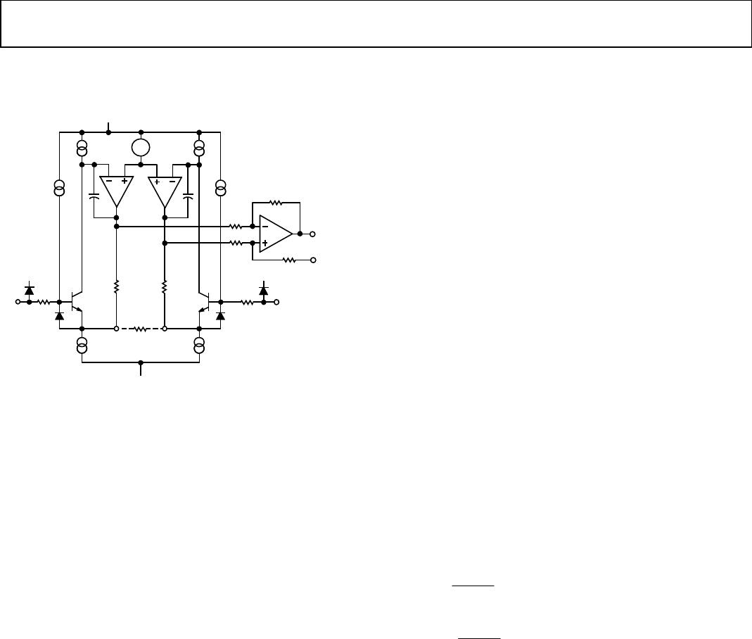
Figure 36. Simplified Schematic of AD620
The AD620 is a monolithic instrumentation amplifier based on
a modification of the classic three op amp approach. Absolute
value trimming allows the user to program gain accurately
(to 0.15% at G = 100) with only one resistor. Monolithic
construction and laser wafer trimming allow the tight matching
and tracking of circuit components, thus ensuring the high level
of performance inherent in this circuit.
The input transistors Q1 and Q2 provide a single differential-
pair bipolar input for high precision (Figure 36), yet offer 10×
lower input bias current thanks to Superϐeta processing.
Feedback through the Q1-A1-R1 loop and the Q2-A2-R2 loop
maintains constant collector current of the input devices Q1
and Q2, thereby impressing the input voltage across the external
gain setting resistor R
G
. This creates a differential gain from the
inputs to the A1/A2 outputs given by G = (R1 + R2)/R
G
+ 1. The
unity-gain subtractor, A3, removes any common-mode signal,
yielding a single-ended output referred to the REF pin potential.
The value of R
G
also determines the transconductance of the
preamp stage. As R
G
is reduced for larger gains, the
transconductance increases asymptotically to that of the input
transistors. This has three important advantages: (a) Open-loop
gain is boosted for increasing programmed gain, thus reducing
gain related errors. (b) The gain-bandwidth product
(determined by C1 and C2 and the preamp transconductance)
increases with programmed gain, thus optimizing frequency
response. (c) The input voltage noise is reduced to a value of
9 nV/√Hz, determined mainly by the collector current and base
resistance of the input devices.
The internal gain resistors, R1 and R2, are trimmed to an
absolute value of 24.7 kΩ, allowing the gain to be programmed
accurately with a single external resistor.
The gain equation is then
1
4.49
+
Ω
=
G
R
k
G
1
4.49
Ω
=
G
k
R
G
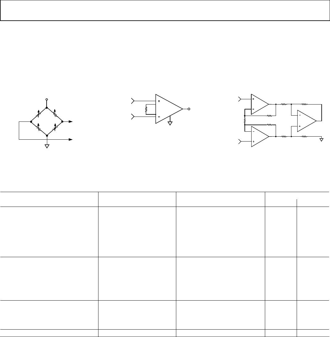
Make vs. Buy: a Typical Bridge Application Error Budget
The AD620 offers improved performance over “homebrew”
three op amp IA designs, along with smaller size, fewer
components, and 10× lower supply current. In the typical
application, shown in Figure 37, a gain of 100 is required to
amplify a bridge output of 20 mV full-scale over the industrial
temperature range of −40°C to +85°C. Table 4 shows how to
calculate the effect various error sources have on circuit
accuracy.
AD620
Rev. H | Page 13 of 20
Regardless of the system in which it is being used, the AD620
provides greater accuracy at low power and price. In simple
systems, absolute accuracy and drift errors are by far the most
significant contributors to error. In more complex systems
with an intelligent processor, an autogain/autozero cycle
removes all absolute accuracy and drift errors, leaving only the
resolution errors of gain, nonlinearity, and noise, thus allowing
full 14-bit accuracy.
Note that for the homebrew circuit, the OP07 specifications for
input voltage offset and noise have been multiplied by √2. This
is because a three op amp type in-amp has two op amps at its
inputs, both contributing to the overall input error.
R = 350
Ω
10V
PRECISION BRIDGE TRANSDUCE
R
R = 350
Ω
R = 350
Ω
R = 350
Ω
00775-0-039
AD620A MONOLITHIC
INSTRUMENTATION
AMPLIFIER, G = 100
SUPPLY CURRENT = 1.3mA MAX
AD620A
R
G
499
Ω
REFERENCE
00775-0-040
Figure 37. Make vs. Buy
"HOMEBREW" IN-AMP, G = 100
*0.02% RESISTOR MATCH, 3ppm/
°
C TRACKING
**DISCRETE 1% RESISTOR, 100ppm/
°
C TRACKING
SUPPLY CURRENT = 15mA MAX
100
Ω
**
10k
Ω
*
10k
Ω
**
10k
Ω
*
10k
Ω
*
10k
Ω
**
10k
Ω
*
OP07D
OP07D
OP07D
00775-0-041
Table 4. Make vs. Buy Error Budget
Error, ppm of Full Scale
Error Source AD620 Circuit Calculation “Homebrew” Circuit Calculation AD620 Homebrew
ABSOLUTE ACCURACY at T
A
= 25°C
Input Offset Voltage, μV 125 μV/20 mV (150 μV × √2)/20 mV 6,250 10,607
Output Offset Voltage, μV 1000 μV/100 mV/20 mV ((150 μV × 2)/100)/20 mV 500 150
Input Offset Current, nA 2 nA ×350 Ω/20 mV (6 nA ×350 Ω)/20 mV 18 53
CMR, dB 110 dB(3.16 ppm) ×5 V/20 mV (0.02% Match × 5 V)/20 mV/100 791 500
Total Absolute Error 7,559 11,310
DRIFT TO 85°C
Gain Drift, ppm/°C (50 ppm + 10 ppm) ×60°C 100 ppm/°C Track × 60°C 3,600 6,000
Input Offset Voltage Drift, μV/°C 1 μV/°C × 60°C/20 mV (2.5 μV/°C × √2 × 60°C)/20 mV 3,000 10,607
Output Offset Voltage Drift, μV/°C 15 μV/°C × 60°C/100 mV/20 mV (2.5 μV/°C × 2 × 60°C)/100 mV/20 mV 450 150
Total Drift Error 7,050 16,757
RESOLUTION
Gain Nonlinearity, ppm of Full Scale 40 ppm 40 ppm 40 40
Typ 0.1 Hz to 10 Hz Voltage Noise, μV p-p 0.28 μV p-p/20 mV (0.38 μV p-p × √2)/20 mV 14 27
Total Resolution Error 54 67
Grand Total Error 14,663 28,134
G = 100, V
S
= ±15 V.
(All errors are min/max and referred to input.)
AD620
Rev. H | Page 14 of 20
3k
Ω
5V
DIGITAL
DATA
OUTPUT
ADC
REF
IN
AGND
20k
Ω
10k
Ω
20k
Ω
AD620B
G = 100
1.7mA 0.10mA
0.6mA
MAX
499
Ω
3k
Ω
3k
Ω
3k
Ω
2
1
8
3
7
6
5
4
1.3mA
MAX
AD705
00775-0-042
Figure 38. A Pressure Monitor Circuit that Operates on a 5 V Single Supply
Pressure Measurement
Although useful in many bridge applications, such as weigh
scales, the AD620 is especially suitable for higher resistance
pressure sensors powered at lower voltages where small size and
low power become more significant.
Figure 38 shows a 3 kΩ pressure transducer bridge powered
from 5 V. In such a circuit, the bridge consumes only 1.7 mA.
Adding the AD620 and a buffered voltage divider allows the
signal to be conditioned for only 3.8 mA of total supply current.
Small size and low cost make the AD620 especially attractive for
voltage output pressure transducers. Since it delivers low noise
and drift, it also serves applications such as diagnostic
noninvasive blood pressure measurement.
Medical ECG
The low current noise of the AD620 allows its use in ECG
monitors (Figure 39) where high source resistances of 1 MΩ or
higher are not uncommon. The AD620’s low power, low supply
voltage requirements, and space-saving 8-lead mini-DIP and
SOIC package offerings make it an excellent choice for battery-
powered data recorders.
Furthermore, the low bias currents and low current noise,
coupled with the low voltage noise of the AD620, improve the
dynamic range for better performance.
The value of capacitor C1 is chosen to maintain stability of
the right leg drive loop. Proper safeguards, such as isolation,
must be added to this circuit to protect the patient from
possible harm.
G = 7
AD620A
0.03Hz
HIGH-
PASS
FILTER
OUTPUT
1V/mV
+3V
–3V
R
G
8.25k
Ω
24.9k
Ω
24.9k
Ω
AD705J
G = 143
C1
1M
Ω
R4
10k
Ω
R1
R3
R2
OUTPUT
AMPLIFIER
PATIENT/CIRCUIT
PROTECTION/ISOLATION
00775-0-043
Figure 39. A Medical ECG Monitor Circuit

AD620BRZ-R7

Mfr. #:
Manufacturer:
Analog Devices Inc.
Description:
Instrumentation Amplifiers AD620 Amplifier Low Drift Low Power
Lifecycle:
New from this manufacturer.
Delivery:
DHL FedEx Ups TNT EMS
Payment:
T/T Paypal Visa MoneyGram Western Union