TCP-4127UB-DT

TCP−4127UB
www.onsemi.com
4
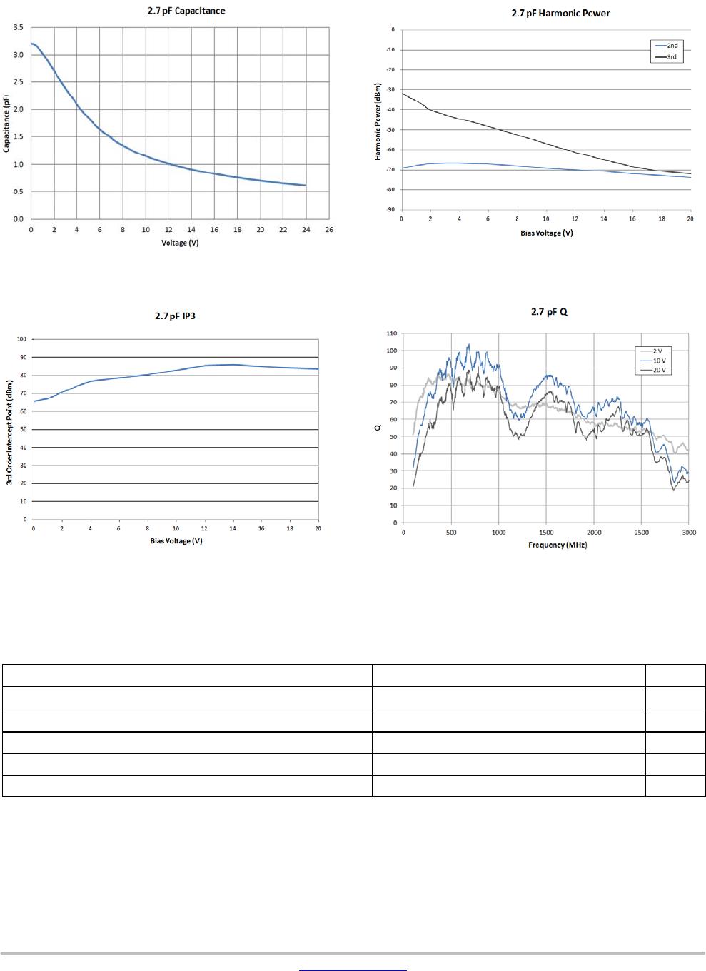
Representative performance data at 255C for 2.7 pF WLCSP Package
Figure 2. Capacitance
Figure 3. Harmonic Power*
Figure 4. IP3* Figure 5. Q*
*Data shown is representative only.
Table 3. ABSOLUTE MAXIMUM RATINGS
Parameter Rating Units
Input Power +40 dBm
Bias Voltage +25 (Note 5) V
Operating Temperature Range −30 to +85 °C
Storage Temperature Range −55 to +125 °C
ESD − Human Body Model Class 1B JEDEC HBM Standard (Note 6)
Stresses exceeding those listed in the Maximum Ratings table may damage the device. If any of these limits are exceeded, device functionality
should not be assumed, damage may occur and reliability may be affected.
5. WLCSP: Recommended Bias Voltage not to exceed 24 V.
6. Class 1B defined as passing 500 V, but may fail after exposure to 1000 V ESD pulse.
TCP−4127UB
www.onsemi.com
5
ASSEMBLY CONSIDERATIONS AND REFLOW PROFILE
The following assembly considerations should be observed:
Cleanliness
These chips should be handled in a clean environment.
Electro-static Sensitivity
ON Semiconductors PTICs are ESD Class 1B sensitive.
The proper ESD handling procedures should be used.
Mounting
The WLCSP PTIC is fabricated for Flip Chip solder
mounting. Connectivity to the RF and Bias terminations on
the PTIC die is established through SAC305 solder balls
with 65 mm nominal height (45 mm to 85 mm height
variation). The PTIC die is RoHS-compliant and compatible
with lead-free soldering profile.
Molding
The PTIC die is compatible for over-molding or
under-fill.
Figure 6. Reflow Profile
ORIENTATION OF THE PTIC FOR OPTIMUM LOSSES
When configuring the PTIC in your specific circuit
design, at least one of the RF terminals must be connected
to DC ground. If minimum transition times are required, DC
ground on both RF terminals is recommended. To minimize
losses, the PTIC should be oriented such that RF2
is at the
lower RF impedance of the two RF nodes. A shunt PTIC, for
example, should have RF2
connected to RF ground.
Figure 7. PTIC Orientation Functional Block
Diagram
Bias
RF ANT
RF1
(PTIC Pad)
RF2
(PTIC Pad)
TCP−4127UB
www.onsemi.com
6
PART NUMBER DEFINITION
Table 4. PART NUMBERS
Part Number
Capacitance
Package*
2 V 24 V
TCP−4127UB-DT 2.70 0.600 4-bump WLCSP
*See PTIC package dimensions on following page.
For information on device numbering and ordering codes,
please download the Device Nomenclature technical note
(TND310/D) from www.onsemi.com
.

TCP-4127UB-DT

Mfr. #:
Manufacturer:
ON Semiconductor
Description:
Tuners GEN 4.1 ULTRA HIGH T
Lifecycle:
New from this manufacturer.
Delivery:
DHL FedEx Ups TNT EMS
Payment:
T/T Paypal Visa MoneyGram Western Union

Products related to this Datasheet