Obsolete Product(s) - Obsolete Product(s)
1
2
4
Vref
ST-BY
7
IN1
C1 0.22µF
V
CC
133
D95AU258A
+
-
-
+
OUT1+
OUT1-
15
14
12
MUTE
6
IN2
C3 0.22µF
+
-
-
+
OUT2+
OUT2-
8
9
S-GND
PW-GND
C5
470µF
C6
100nF
R1 10K
C2
10µF
µP
R2 10K
C4
1µF
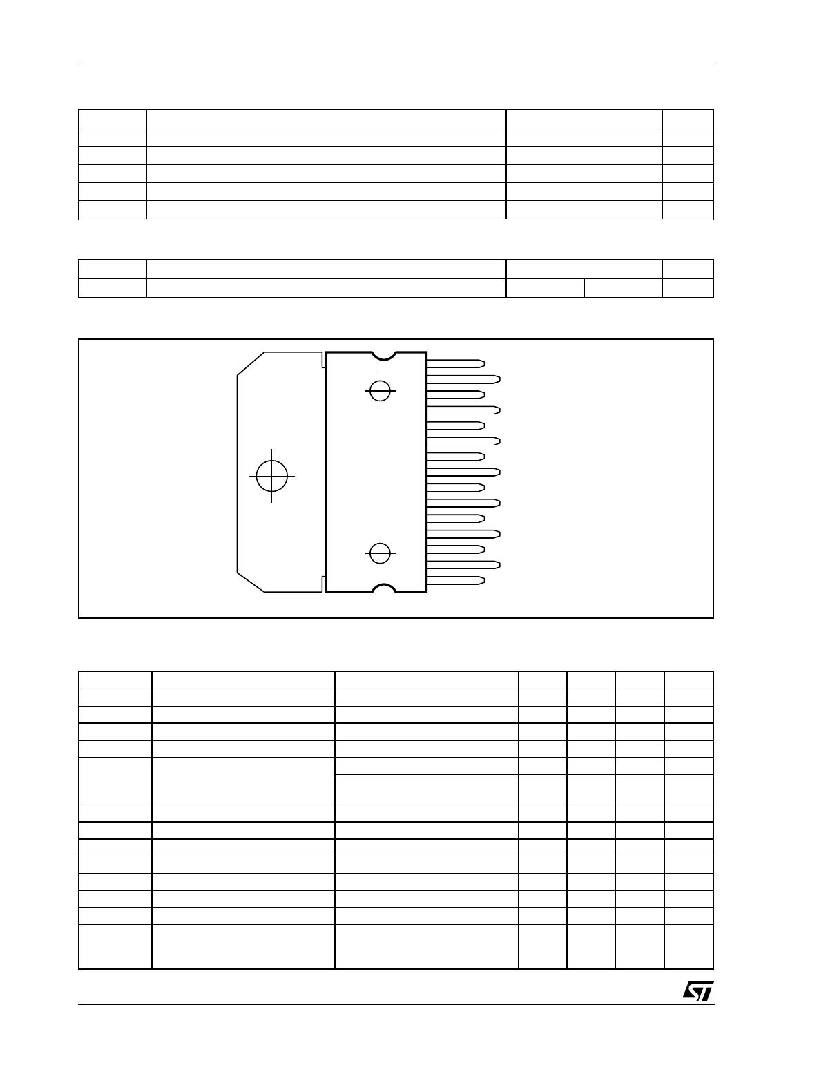
Figure 1:
Microprocessor Application
ELECTRICAL CHARACTERISTICS
(Continued)
Symbol Parameter Test Condition Min. Typ. Max. Unit
VT
ST-BY
St-by Threshold 0.8 1.3 1.8 V
I
ST-BY
ST-BY current V6 = GND 100 µA
e
N
Total Output Noise Voltage A curve
f = 20Hz to 20kHz
150 µV
APPLICATION SUGGESTION
STAND-BY AND MUTE FUNCTIONS
(A) Microprocessor Application
In order to avoid annoying "Pop-Noise" during
Turn-On/Off transients, it is necessary to guaran-
tee the right St-by and mute signals sequence.
It is quite simple to obtain this function using a mi-
croprocessor (Fig. 1 and 2).
At first St-by signal (from mP) goes high and the
voltage across the St-by terminal (Pin 7) starts to
increase exponentially. The external RC network
is intended to turn-on slowly the biasing circuits of
the amplifier, this to avoid "POP" and "CLICK" on
the outputs.
When this voltage reaches the St-by threshold
level, the amplifier is switched-on and the external
capacitors in series to the input terminals (C3,
C5) start to charge.
It’s necessary to mantain the mute signal low until
the capacitors are fully charged, this to avoid that
the device goes in play mode causing a loud "Pop
Noise" on the speakers.
A delay of 100-200ms between St-by and mute
signals is suitable for a proper operation.
TDA7266S
3/8
Obsolete Product(s) - Obsolete Product(s)