MC100EP90DTR2G

MC10EP90, MC100EP90
http://onsemi.com
4
Table 5. 10EP DC CHARACTERISTICS V
CC
= 3.3 V, V
EE
= −5.5 V to −3.0 V; GND = 0 V (Note 2)
Symbo
l
Characteristic
−40°C 25°C 85°C
Unit
Min Typ Max Min Typ Max Min Typ Max
I
EE
Negative Power Supply Current 5 13 20 5 13 20 5 13 20 mA
I
CC
Positive Power Supply Current 43 55 67 43 55 67 43 55 67 mA
V
OH
Output HIGH Voltage (Note 3) 2165 2290 2415 2230 2355 2480 2290 2415 2540 mV
V
OL
Output LOW Voltage (Note 3) 1365 1490 1615 1430 1555 1680 1490 1615 1740 mV
V
IH
Input HIGH Voltage (Single−Ended) −1210 −885 −1145 −820 −1085 −760 mV
V
IL
Input LOW Voltage (Single−Ended) −1935 −1610 −1870 −1545 −1810 −1485 mV
V
BB
Output Voltage Reference −1510 −1410 −1310 −1445 −1345 −1245 −1385 −1285 −1185 mV
V
IHCMR
Input HIGH Voltage Common Mode
Range (Differential Configuration)
(Note 4)
V
EE
+2.0 0.0 V
EE
+2.0 0.0 V
EE
+2.0 0.0 V
I
IH
Input HIGH Current 150 150 150
mA
I
IL
Input LOW Current 0.5 0.5 0.5
mA
NOTE: Device will meet the specifications after thermal equilibrium has been established when mounted in a test socket or printed circuit
board with maintained transverse airflow greater than 500 lfpm. Electrical parameters are guaranteed only over the declared
operating temperature range. Functional operation of the device exceeding these conditions is not implied. Device specification limit
values are applied individually under normal operating conditions and not valid simultaneously.
2. Input and output parameters vary 1:1 with V
CC
.
3. All loading with 50 W to V
CC
− 2.0 V.
4. V
IHCMR
min varies 1:1 with V
EE
, max varies 1:1 with V
CC
. The V
IHCMR
range is referenced to the most positive side of the differential input
signal.
Table 6. 10EP DC CHARACTERISTICS V
CC
= 5.0 V, V
EE
= −5.5 V to −3.0 V; GND = 0 V (Note 5)
Symbo
l
Characteristic
−40°C 25°C 85°C
Unit
Min Typ Max Min Typ Max Min Typ Max
I
EE
Negative Power Supply Current 5 13 20 5 13 20 5 13 20 mA
I
CC
Positive Power Supply Current 43 55 67 43 55 67 43 55 67 mA
V
OH
Output HIGH Voltage (Note 6) 3865 3990 4115 3930 4055 4180 3990 4115 4240 mV
V
OL
Output LOW Voltage (Note 6) 3065 3190 3315 3130 3255 3380 3190 3315 3440 mV
V
IH
Input HIGH Voltage (Single−Ended) −1210 −885 −1145 −820 −1085 −760 mV
V
IL
Input LOW Voltage (Single−Ended) −1935 −1610 −1870 −1545 −1810 −1485 mV
V
BB
Output Voltage Reference −1510 −1410 −1310 −1445 −1345 −1245 −1385 −1285 −1185 mV
V
IHCMR
Input HIGH Voltage Common Mode
Range (Differential Configuration)
(Note 7)
V
EE
+2.0 0.0 V
EE
+2.0 0.0 V
EE
+2.0 0.0 V
I
IH
Input HIGH Current 150 150 150
mA
I
IL
Input LOW Current 0.5 0.5 0.5
mA
NOTE: Device will meet the specifications after thermal equilibrium has been established when mounted in a test socket or printed circuit
board with maintained transverse airflow greater than 500 lfpm. Electrical parameters are guaranteed only over the declared
operating temperature range. Functional operation of the device exceeding these conditions is not implied. Device specification limit
values are applied individually under normal operating conditions and not valid simultaneously.
5. Input and output parameters vary 1:1 with V
CC
.
6. All loading with 50 W to V
CC
− 2.0 V.
7. V
IHCMR
min varies 1:1 with V
EE
, max varies 1:1 with V
CC
. The V
IHCMR
range is referenced to the most positive side of the differential input
signal.
MC10EP90, MC100EP90
http://onsemi.com
5
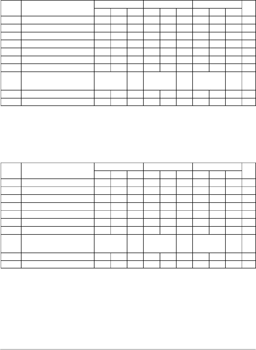
Table 7. 100EP DC CHARACTERISTICS V
CC
= 3.3 V, V
EE
= −5.5 V to −3.0 V; GND = 0 V (Note 8)
Symbo
l
Characteristic
−40°C 25°C 85°C
Unit
Min Typ Max Min Typ Max Min Typ Max
I
EE
Negative Power Supply Current 5 13 20 5 13 20 5 13 20 mA
I
CC
Positive Power Supply Current 45 58 70 50 62 75 53 65 78 mA
V
OH
Output HIGH Voltage (Note 9) 2155 2280 2405 2155 2280 2405 2155 2280 2405 mV
V
OL
Output LOW Voltage (Note 9) 1305 1480 1605 1305 1480 1605 1305 1480 1605 mV
V
IH
Input HIGH Voltage (Single−Ended) −1225 −885 −1225 −885 −1225 −885 mV
V
IL
Input LOW Voltage (Single−Ended) −1995 −1625 −1995 −1625 −1995 −1625 mV
V
BB
Output Voltage Reference −1525 −1425 −1325 −1525 −1425 −1325 −1525 −1425 −1325 mV
V
IHCMR
Input HIGH Voltage Common Mode
Range (Differential Configuration)
(Note 10)
V
EE
+2.0 0.0 V
EE
+2.0 0.0 V
EE
+2.0 0.0 V
I
IH
Input HIGH Current 150 150 150
mA
I
IL
Input LOW Current 0.5 0.5 0.5
mA
NOTE: Device will meet the specifications after thermal equilibrium has been established when mounted in a test socket or printed circuit
board with maintained transverse airflow greater than 500 lfpm. Electrical parameters are guaranteed only over the declared
operating temperature range. Functional operation of the device exceeding these conditions is not implied. Device specification limit
values are applied individually under normal operating conditions and not valid simultaneously.
8. Input and output parameters vary 1:1 with V
CC
.
9. All loading with 50 W to V
CC
− 2.0 V.
10.V
IHCMR
min varies 1:1 with V
EE
, max varies 1:1 with V
CC
. The V
IHCMR
range is referenced to the most positive side of the differential input
signal.
Table 8. 100EP DC CHARACTERISTICS V
CC
= 5.0 V, V
EE
= −5.5 V to −3.0 V; GND = 0 V (Note 11)
Symbo
l
Characteristic
−40°C 25°C 85°C
Unit
Min Typ Max Min Typ Max Min Typ Max
I
EE
Negative Power Supply Current 5 13 20 5 13 20 5 13 20 mA
I
CC
Positive Power Supply Current 45 58 70 50 62 75 53 65 78 mA
V
OH
Output HIGH Voltage (Note 12) 3855 3980 4105 3855 3980 4105 3855 3980 4105 mV
V
OL
Output LOW Voltage (Note 12) 3005 3180 3305 3005 3180 3305 3005 3180 3305 mV
V
IH
Input HIGH Voltage (Single−Ended) −1225 −885 −1225 −885 −1225 −885 mV
V
IL
Input LOW Voltage (Single−Ended) −1995 −1625 −1995 −1625 −1995 −1625 mV
V
BB
Output Voltage Reference −1525 −1425 −1325 −1525 −1425 −1325 −1525 −1425 −1325 mV
V
IHCMR
Input HIGH Voltage Common Mode
Range (Differential Configuration)
(Note 13)
V
EE
+2.0 0.0 V
EE
+2.0 0.0 V
EE
+2.0 0.0 V
I
IH
Input HIGH Current 150 150 150
mA
I
IL
Input LOW Current 0.5 0.5 0.5
mA
NOTE: Device will meet the specifications after thermal equilibrium has been established when mounted in a test socket or printed circuit
board with maintained transverse airflow greater than 500 lfpm. Electrical parameters are guaranteed only over the declared
operating temperature range. Functional operation of the device exceeding these conditions is not implied. Device specification limit
values are applied individually under normal operating conditions and not valid simultaneously.
11. Input and output parameters vary 1:1 with V
CC
.
12.All loading with 50 W to V
CC
− 2.0 V.
13.V
IHCMR
min varies 1:1 with V
EE
, max varies 1:1 with V
CC
.. The V
IHCMR
range is referenced to the most positive side of the differential input
signal.
MC10EP90, MC100EP90
http://onsemi.com
6
Table 9. AC CHARACTERISTICS V
EE
= −3.0 V to −5.5 V; V
CC
= 3.0 V to 5.5 V; GND = 0 V (Note 14)
Symbo
l
Characteristic
−40°C 25°C 85°C
Unit
Min Typ Max Min Typ Max Min Typ Max
f
max
Maximum Frequency
(See Figure 2 F
max
/JITTER)
> 3 > 3 > 3 GHz
t
PLH
,
t
PHL
Propagation Delay to
Output Differential
170 240 310 200 260 340 230 300 370 ps
t
SKEW
Duty Cycle Skew (Note 15) 5.0 20 5.0 20 5.0 20
ps
Within Device Skew Q, Q
Device to Device Skew (Note 15)
80
140
80
140
80
140
t
JITTER
Cycle−to−Cycle Jitter
(See Figure 2 F
max
/JITTER)
0.2 < 1 0.2 < 1 0.2 < 1 ps
V
PP
Input Voltage
Swing (Differential Configuration)
150 800 1200 150 800 1200 150 800 1200 mV
t
r
t
f
Output Rise/Fall Times Q, Q
(20% − 80%)
70 120 170 80 130 180 100 150 230 ps
NOTE: Device will meet the specifications after thermal equilibrium has been established when mounted in a test socket or printed circuit
board with maintained transverse airflow greater than 500 lfpm. Electrical parameters are guaranteed only over the declared
operating temperature range. Functional operation of the device exceeding these conditions is not implied. Device specification limit
values are applied individually under normal operating conditions and not valid simultaneously.
14.Measured using a 750 mV source, 50% duty cycle clock source. All loading with 50 W to V
CC
−2.0 V.
15.Skew is measured between outputs under identical transitions. Duty cycle skew is defined only for differential operation when the delays
are measured from the cross point of the inputs to the cross point of the outputs.
0
100
200
300
400
500
600
700
800
900
0 1000 2000 3000 4000 5000
Figure 2. F
max
/Jitter
FREQUENCY (MHz)
1
2
3
4
5
6
7
8
(JITTER)
9
V
OUTpp
(mV)
JITTER
OUT
ps (RMS)

MC100EP90DTR2G

Mfr. #:
Manufacturer:
ON Semiconductor
Description:
Translation - Voltage Levels 3.3V/5V Triple ECL to LVPECL/PECL
Lifecycle:
New from this manufacturer.
Delivery:
DHL FedEx Ups TNT EMS
Payment:
T/T Paypal Visa MoneyGram Western Union