ZL30321 Short Form Data Sheet
8
Zarlink Semiconductor Inc.
2.0 Overview
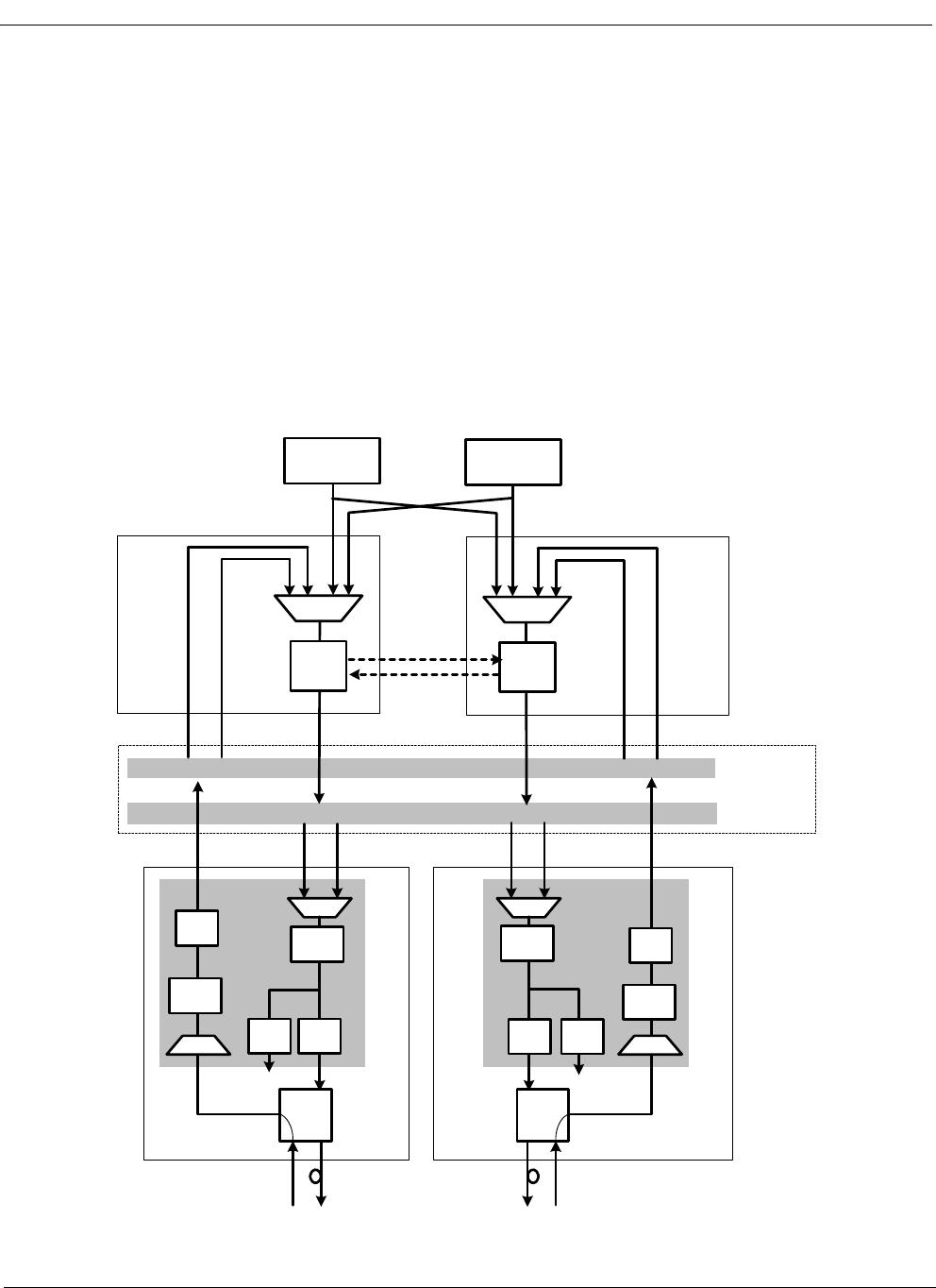
The ZL30321 SONET/SDH/GbE Mulit-Rate Line Card Synchronizer is a highly integrated device that provides
timing for network interface cards. It incorporates two independent DPLLs, each capable of locking to one of eight
input references and provides a wide variety of synchronized output clocks and frame pulses.
This device is ideally suited for designs that require both a transmit timing path (backplane to PHY) and a receive
timing path (PHY to backplane). Each path is controlled with separate DPLLs (DPLL1, DPLL1) which are both
independently configurable through the serial interface (SPI or I
2
C). A typical application of the ZL30321 is shown
in Figure 2. In this application, the ZL30321 translates the 19.44 MHz clock from the telecom rate backplane
(system timing bus), translates the frequency to 125 MHz for the PHY Tx clock, and filters the jitter to ensure
compliance with the related standards. A programmable synthesizer (P0) provides optional synchronous PDH
clocks with multiples of 8 kHz for generating PDH interface clocks. On the receive path, DPLL2 and the P1
synthesizer translate the line recovered clock (8 kHz or 1.544 MHz) from the PHY to the 19.44 MHz telecom
backplane (line recovered timing) for the central timing cards. The ZL30321 allows easy integration of Ethernet line
rates with today’s telecom backplanes.
Figure 2 - Typical Application of the ZL30321
Line Recovered Timing
System Timing Bus
19.44 MHz 19.44 MHz
19.44 MHz
ZL30321
APLL
A
B
125 MHz
Ethernet
Line Card
PHY
8 kHz
Telecom
Backplane
ZL30321
A
B
T1/E1
Line Card
PHY
1.544 MHz
S
19.44 MHz
P
Central
Timing
Card
BITS A
PS
PS
A
DPLL
Central
Timing
Card
BITS B
PS
PS
B
DPLL
XOVER
ZL30121
ZL30121
P1
P1
P0
P0
DPLL1
DPLL1
DPLL2
DPLL2
APLL
1.544 MHz
and/or
2.048 MHz

