2
COMMERCIAL AND INDUSTRIAL TEMPERATURE RANGES
IDT2308
3.3V ZERO DELAY CLOCK MULTIPLIER
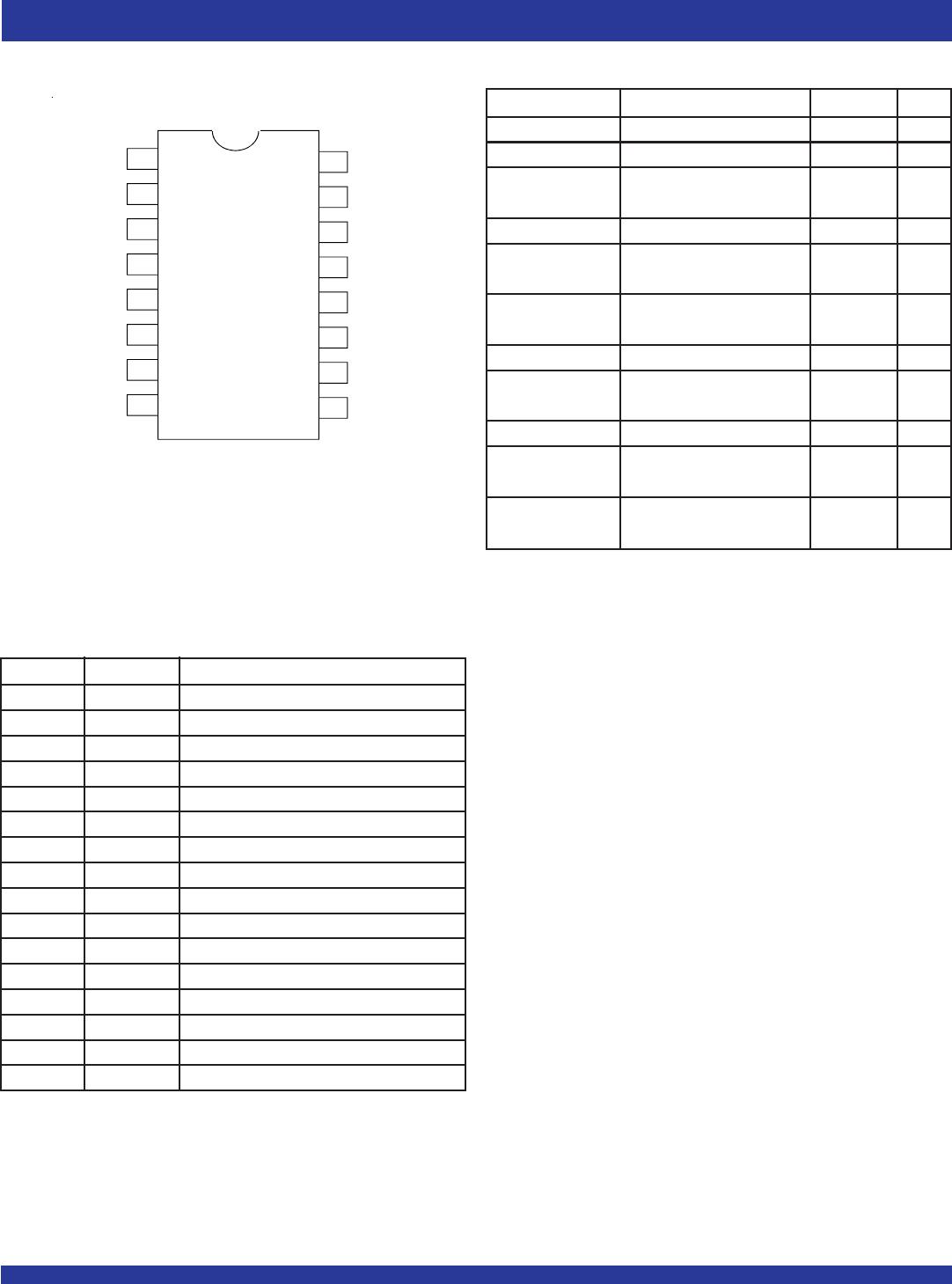
PIN CONFIGURATION
SOIC/ TSSOP
TOP VIEW
REF
CLKA1
S2
2
3
4
5
6
7
8
9
10
11
12
13
14
15
161
CLKA2
GND
CLKB1
FBK
CLKA4
GND
S1
V
DD
VDD
CLKB2
CLKB3
CLKB4
CLKA3
Symbol Rating Max. Unit
VDD Supply Voltage Range –0.5 to +4.6 V
VI
(2)
Input Voltage Range (REF) –0.5 to +5.5 V
V
I Input Voltage Range –0.5 to V
(except REF) VDD+0.5
IIK (VI < 0) Input Clamp Current –50 mA
I
OK Terminal Voltage with Respect ±50 mA
(VO < 0 or VO > VDD) to GND (inputs VIH 2.5, VIL 2.5)
I
O Continuous Output Current ±50 mA
(VO = 0 to VDD)
VDD or GND Continuous Current ±100 mA
T
A = 55°C Maximum Power Dissipation 0.7 W
(in still air)
(3)
TSTG Storage Temperature Range –65 to +150 ° C
Operating Commercial Temperature 0 to +70 °C
Temperature Range
Operating Industrial Temperature -40 to +85 °C
Temperature Range
NOTES:
1. Stresses greater than those listed under ABSOLUTE MAXIMUM RATINGS may
cause permanent damage to the device. This is a stress rating only and functional
operation of the device at these or any other conditions above those indicated in the
operational sections of this specification is not implied. Exposure to absolute maximum
rating conditions for extended periods may affect reliability.
2. The input and output negative-voltage ratings may be exceeded if the input and output
clamp-current ratings are observed.
3. The maximum package power dissipation is calculated using a junction temperature
of 150°C and a board trace length of 750 mils.
APPLICATIONS:
• SDRAM
• Telecom
• Datacom
• PC Motherboards/Workstations
• Critical Path Delay Designs
Pin Number Functional Description
REF 1 Input Reference Clock, 5 Volt Tolerant Input
CLKA1
(1)
2 Clock Output for Bank A
CLKA2
(1)
3 Clock Output for Bank A
VDD 4 3.3V Supply
GND 5 Ground
CLKB1
(1)
6 Clock Output for Bank B
CLKB2
(1)
7 Clock Output for Bank B
S2
(2)
8 Select Input, Bit 2
S1
(2)
9 Select Input, Bit 1
CLKB3
(1)
10 Clock Output for Bank B
CLKB4
(1)
11 Clock Output for Bank B
GND 12 Ground
VDD 13 3.3V Supply
CLKA3
(1)
14 Clock Output for Bank A
CLKA4
(1)
15 Clock Output for Bank A
FBK 16 PLL Feedback Input
NOTES:
1. Weak pull down on all outputs.
2. Weak pull ups on these inputs.
PIN DESCRIPTION
ABSOLUTE MAXIMUM RATINGS
(1)