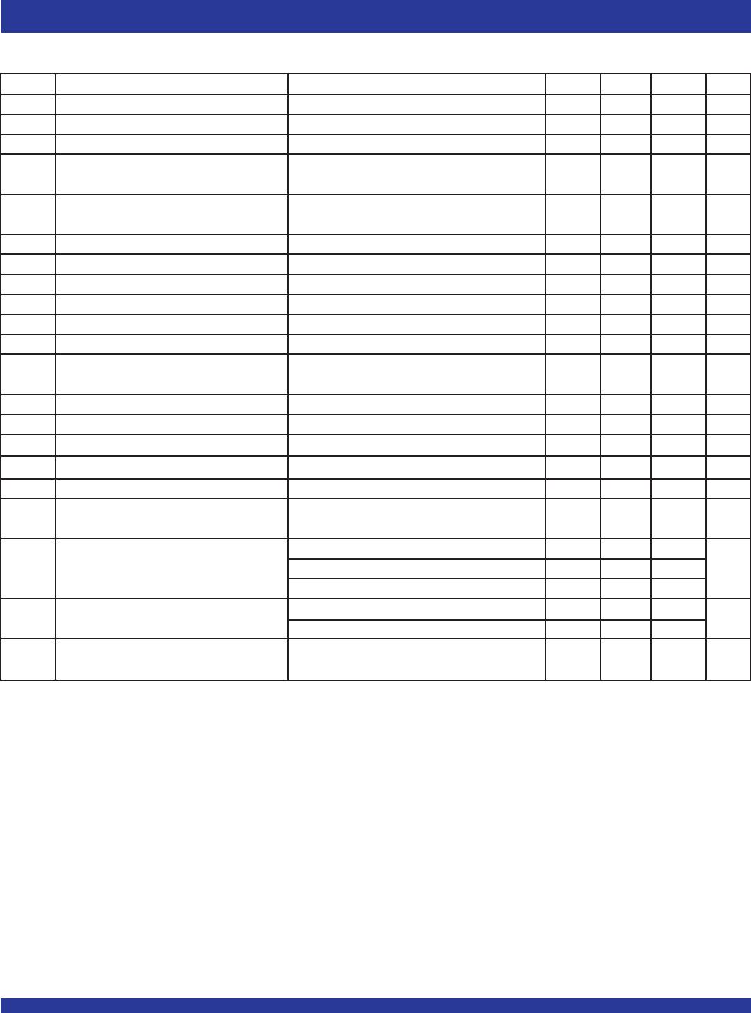
4
COMMERCIAL AND INDUSTRIAL TEMPERATURE RANGES
IDT2308
3.3V ZERO DELAY CLOCK MULTIPLIER
ZERO DELAY AND SKEW CONTROL
To close the feedback loop of the IDT2308, the FBK pin can be driven from any of the eight available output pins. The output driving the FBK pin will
be driving a total load of 7pF plus any additional load that it drives. The relative loading of this output (with respect to the remaining outputs) can adjust
the input-output delay.
For applications requiring zero input-output delay, all outputs including the one providing feedback should be equally loaded. If input-output delay
adjustments are required, use the Output Load Difference Chart to calculate loading differences between the feedback output and remaining outputs.
Ensure the outputs are loaded equally, for zero output-output skew.
REF TO CLKA/CLKB DELAY vs. OUTPUT LOAD DIFFERENCE BETWEEN FBK PIN AND CLKA/CLKB PINS
REF to CLKA/CLKB Delay (ps)
OUTPUT LOAD DIFFERENCE BETWEEN FBK PIN AND CLKA/CLKB PINS ( pF)
1500
1000
500
0
-500
-1000
-1500
-30 -25 -20
-15
-10
-5
05
10 15 20 25
30
5
COMMERCIAL AND INDUSTRIAL TEMPERATURE RANGES
IDT2308
3.3V ZERO DELAY CLOCK MULTIPLIER
NOTES:
1. Applies to both REF and FBK.
2. The IDT2308 requires a monotonic ramp-up of the V
DD supply during power up of the
device.
DC ELECTRICAL CHARACTERISTICS - COMMERCIAL
Symbol Parameter Conditions Min. Typ.
(1)
Max. Unit
VIL Input LOW Voltage Level 0.8 V
VIH Input HIGH Voltage Level 2 V
IIL Input LOW Current VIN = 0V 50 μA
IIH Input HIGH Current VIN = VDD ——100μA
VOL Output LOW Voltage IOL = 8mA (-1, -2, -3, -4) 0.4 V
IOL = 12mA (-1H, -2H, -5H)
VOH Output HIGH Voltage IOH = -8mA (-1, -2, -3, -4) 2.4 V
IOH = -12mA (-1H, -2H, -5H)
IDD_PD Power Down Current REF = 0MHz (S2 = S1 = H) 12 μA
100MHz CLKA (-1, -2, -3, -4) 45
100MHz CLKA (-1H, -2H, -5H) 70
IDD Supply Current Unloaded Outputs 66MHz CLKA (-1, -2, -3, -4) 32 mA
Select Inputs at VDD or GND 66MHz CLKA (-1H, -2H, -5H) 50
33MHz CLKA (-1, -2, -3, -4) 18
33MHz CLKA (-1H, -2H, -5H) 30
Symbol Parameter Test Conditions Min. Max. Unit
VDD Supply Voltage
[2]
3 3.6 V
TA Operating Temperature (Ambient Temperature) 0 70 °C
CL Load Capacitance below 100MHz 30 pF
Load Capacitance from 100MHz to 133MHz 15 pF
C
IN Input Capacitance
(1)
—7pF
OPERATING CONDITIONS- COMMERCIAL
6
COMMERCIAL AND INDUSTRIAL TEMPERATURE RANGES
IDT2308
3.3V ZERO DELAY CLOCK MULTIPLIER
SWITCHING CHARACTERISTICS - COMMERCIAL
Symbol Parameter Conditions Min. Typ. Max. Unit
t1 Output Frequency 30pF Load, all devices 10 100 MHz
t1 Output Frequency 20pF Load, -1H, -2H, -5H Devices
(1)
10 133.3 M H z
t1 Output Frequency 15pF Load, -1, -2, -3, -4 devices 10 133.3 M H z
Duty Cycle = t
2 ÷ t1 Measured at 1.4V, FOUT = 66.66MHz 40 50 60 %
(-1, -2, -3, -4, -1H, -2H, -5H) 30pF Load
Duty Cycle = t
2 ÷ t1 Measured at 1.4V, FOUT = 50MHz 45 50 55 %
(-1, -2, -3, -4, -1H, -2H, -5H) 15pF Load
t3 Rise Time (-1, -2, -3, -4) Measured between 0.8V and 2V, 30pF Load 2.2 ns
t3 Rise Time (-1, -2, -3, -4) Measured between 0.8V and 2V, 15pF Load 1.5 ns
t3 Rise Time (-1H, -2H, -5H) Measured between 0.8V and 2V, 30pF Load 1.5 ns
t4 Fall Time (-1, -2, -3, -4) Measured between 0.8V and 2V, 30pF Load 2.2 ns
t4 Fall Time (-1, -2, -3, -4) Measured between 0.8V and 2V, 15pF Load 1.5 ns
t4 Fall Time (-1H, -5H) Measured between 0.8V and 2V, 30pF Load 1.25 ns
t5 Output to Output Skew on same Bank All outputs equally loaded 200 ps
(-1, -2, -3, -4)
Output to Output Skew (-1H, -2H, -5H) All outputs equally loaded 200 ps
Output Bank A to Output Bank B (-1, -4, -2H, -5H) All outputs equally loaded 200 ps
Output Bank A to Output Bank B Skew (-2, -3) All outputs equally loaded 400 ps
t6 Delay, REF Rising Edge to FBK Rising Edge Measured at VDD/2 0 ±250 ps
t7 Device to Device Skew Measured at VDD/2 on the FBK pins of devices 0 700 ps
t8 Output Slew Rate Measured between 0.8V and 2V on -1H, -2H, -5H 1 V/ns
device using Test Circuit 2
tJ Cycle to Cycle Jitter Measured at 66.67 MHz, loaded outputs, 15pF Load 200
(-1, -1H, -4, -5H) Measured at 66.67 MHz, loaded outputs, 30pF Load 200 ps
Measured at 133.3 MHz, loaded outputs, 15pF Load 100
tJ Cycle to Cycle Jitter Measured at 66.67 MHz, loaded outputs, 30pF Load 400 ps
(-2, -2H, -3) Measured at 66.67 MHz, loaded outputs, 15pF Load 400
tLOCK PLL Lock Time Stable Power Supply, valid clocks presented 1 ms
on REF and FBK pins
NOTE:
1. IDT2308-5H has maximum input frequency of 133.33 MHz and maximum output of 66.67MHz.

2308-2DCGI

Mfr. #:
Manufacturer:
IDT
Description:
Clock Generators & Support Products 3.3V PLL ZERO DELAY CLOCK MULTIPLIER
Lifecycle:
New from this manufacturer.
Delivery:
DHL FedEx Ups TNT EMS
Payment:
T/T Paypal Visa MoneyGram Western Union