NCP1075A/B, NCP1076A/B, NCP1077A/B, NCP1079A/B
www.onsemi.com
19
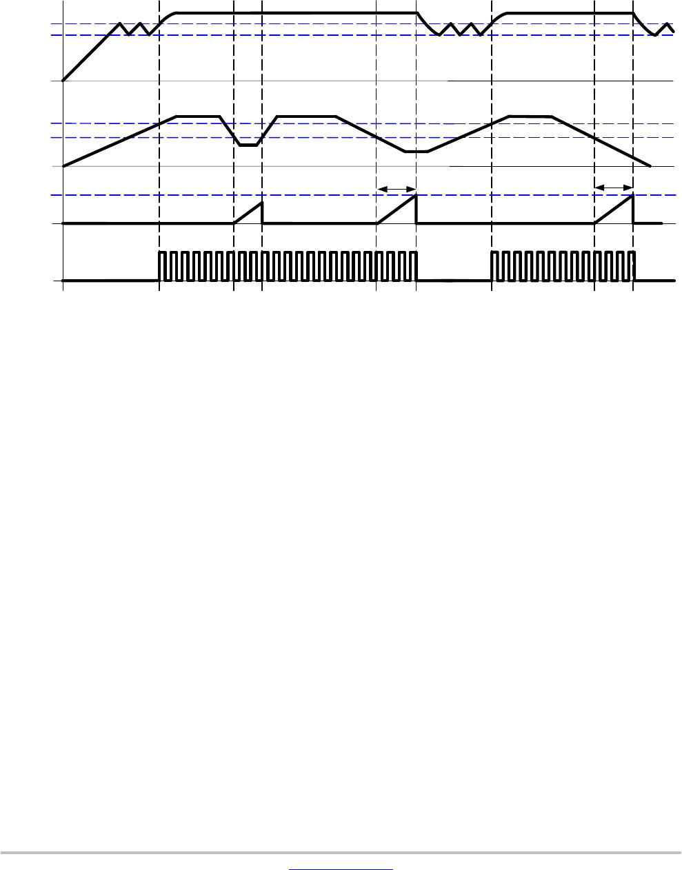
Jittering
Frequency jittering is a method used to soften the EMI
signature by spreading the energy in the vicinity of the main
switching component. The NCP107xu offers a ±6%
deviation of the nominal switching frequency. The sweeping
sawtooth is internally generated and modulates the clock up
and down with a fixed frequency of 300 Hz. Figure 39 shows
the relationship between the jitter ramp and the frequency
deviation. It is not possible to externally disable the jitter.
65 kHz
68.9 kHz
61.1 kHz
Jitter ramp
Internal
sawtooth
adjustable
Figure 39. Modulation Effects on the Clock Signal by the Jittering Sawtooth
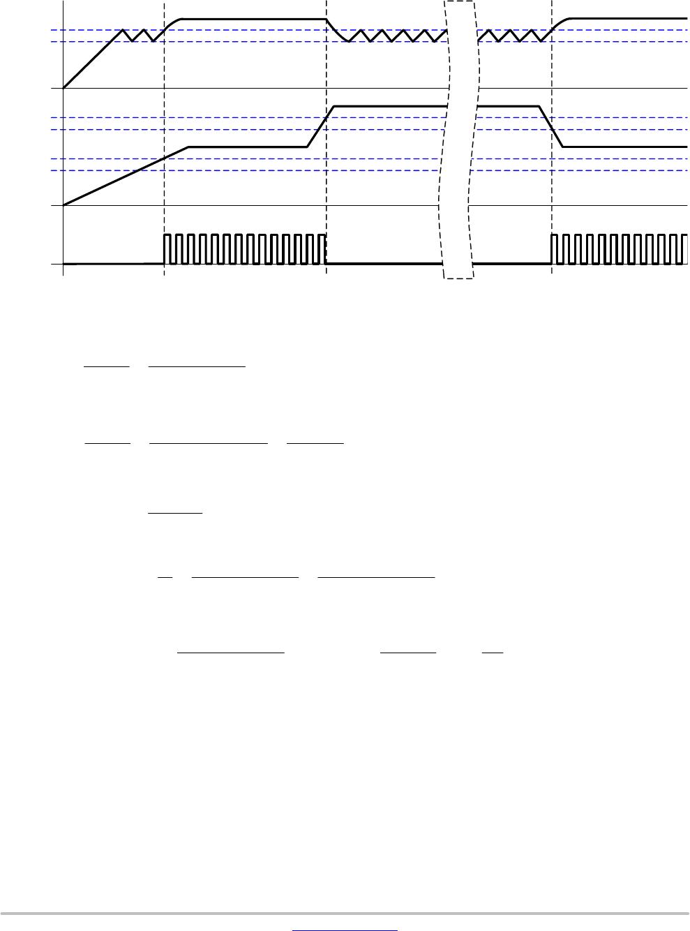
Line Detection
When BO/AC_OVP pin is grounded (voltage on this pin
is below V
BO(EN)
) Figure 2, then an internal comparator
monitors the drain voltage as recovering from one of the
following situations:
• Short−Circuit Protection,
• V
CC
OVP is Confirmed,
• UVLO
• TSD
If the drain voltage is lower than the internal threshold
V
HV(EN)
(91 V dc typically), the internal power switch is
inhibited. This avoids operating at too low ac input.
Brown−out Function, Ac Line Over−voltage Protection
The Brown−out circuitry offers a way to protect the
application from operation under too low an input voltage.
Below a given level, the controller blocks the output pulses,
above it, it authorizes them. The internal circuitry, depicted
by Figure 40, offers a way to observe the high−voltage (HV)
rail.
Figure 40. The Internal Brown−out Configuration
BO/AC_OVP
V
BO(ON)
V
BO(EN)
Line
detection
disable
BO enable
V
AC(OVP)
AC OVP
20μs
filter
20μs
filter
20μs
filter
R
UPPER
R
LOWER
V
BULK
C
BO
t
BO