NCP1075A/B, NCP1076A/B, NCP1077A/B, NCP1079A/B
www.onsemi.com
6
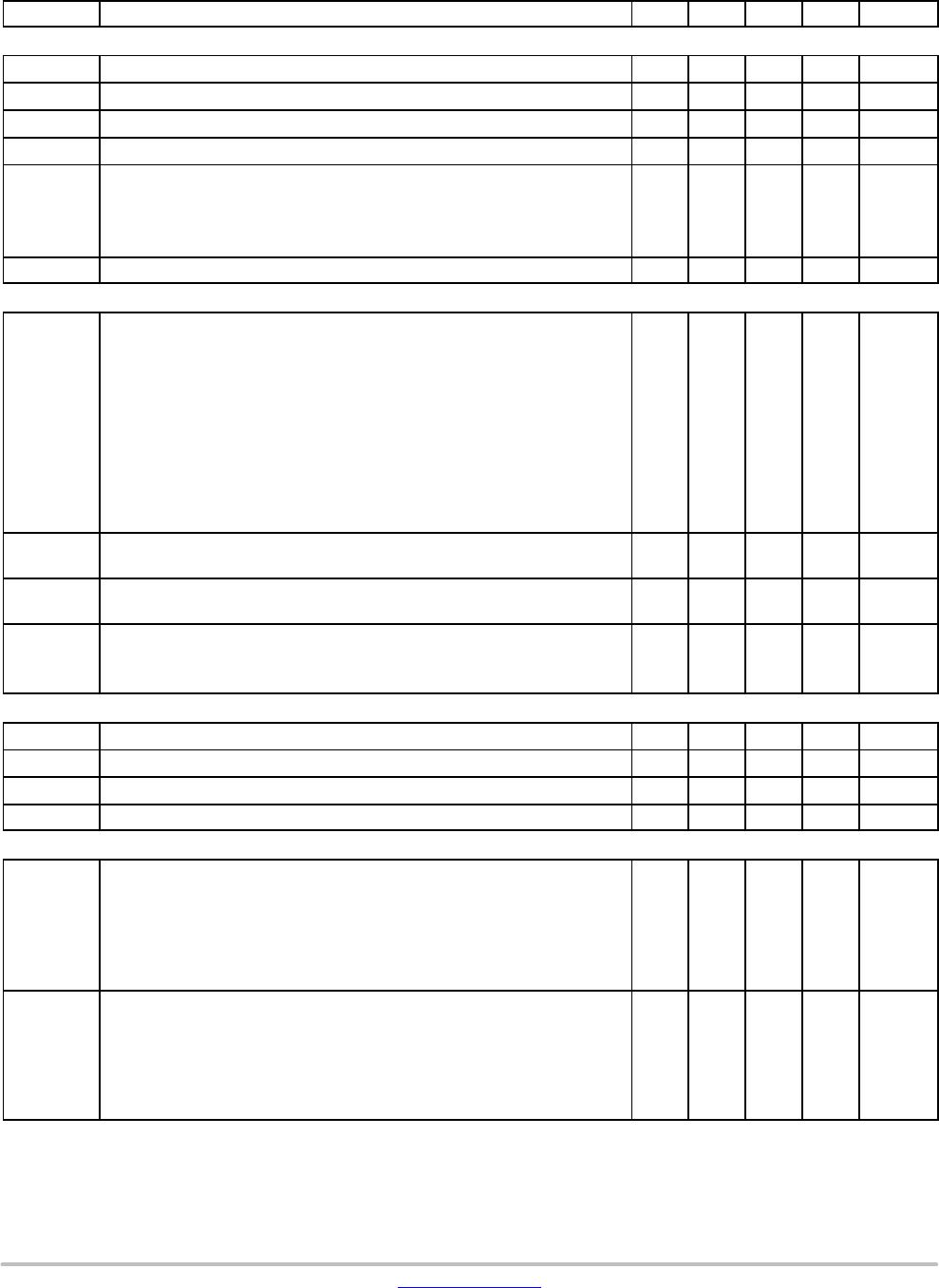
ELECTRICAL CHARACTERISTICS
(For typical values T
J
= 25°C, for min/max values T
J
= −40°C to +125°C, V
CC
= 12 V unless otherwise noted)
Symbol Rating Pin Min Typ Max Unit
SUPPLY SECTION AND VCC MANAGEMENT
V
CC(ON)
V
CC
increasing level at which the switcher starts operation 1 (2) 8.0 8.4 8.9 V
V
CC(MIN)
V
CC
decreasing level at which the HV current source restarts 1 (2) 6.5 6.9 7.3 V
V
CC(OFF)
V
CC
decreasing level at which the switcher stops operation (UVLO) 1 (2) 6.1 6.5 6.9 V
V
CC(reset)
V
CC
voltage at which the internal latch is reset (Guaranteed by design) 1 (2) 4 V
I
CC1
Internal IC consumption, MOSFET switching (f
SW
= 65 kHz)
NCP1075u
NCP1076u/77u
NCP1079u
1 (2)
−
−
−
1.10
1.26
1.40
−
−
−
mA
I
CC(skip)
Internal IC consumption, V
FB
is 0 V (No switching on MOSFET) 1 (2) − 400 −
mA
POWER SWITCH CIRCUIT
R
DS(ON)
Power Switch Circuit on−state resistance (I
DRAIN
= 50 mA)
NCP1075u
T
J
= 25°C
T
J
= 125°C
NCP1076u/77u
T
J
= 25°C
T
J
= 125°C
NCP1079u
T
J
= 25°C
T
J
= 125°C
5 (4)
−
−
−
−
−
−
13.5
26.0
4.8
9.3
2.9
5.3
16.8
31.6
6.8
11.6
3.9
7.5
W
BV
DSS
Power Switch Circuit & Start−up breakdown voltage
(I
DRAIN(OFF)
= 120 mA, T
J
= 25°C)
5 (4) 700 − − V
I
DSS(OFF)
Power Switch & Start−up breakdown voltage off−state leakage current
T
J
= 125°C (V
DS
= 700 V)
5 (4) − 85 −
mA
t
R
t
F
Switching characteristics (R
L
= 50 W, V
DS
set for I
DRAIN
= 0.7 x I
lim
)
Turn−on time (90% − 10%)
Turn−off time (10% − 90%)
5 (4)
−
−
20
10
−
−
ns
INTERNAL START−UP CURRENT SOURCE
I
start1
High−voltage current source, V
CC
= V
CC(ON)
– 200 mV 5 (4) 4.0 9.0 12.0 mA
I
start2
High−voltage current source, V
CC
= 0 V 5 (4) − 0.5 − mA
V
HV(MIN)
Minimum start−up voltage, V
CC
= 0 V 5 (4) − 21 − V
V
CC(TH)
V
CC
Transient level for I
start1
to I
start2
toggling point 1 (2) − 1.6 − V
CURRENT COMPARATOR
I
PK
Maximum internal current set−point at 50% duty−cycle
FB pin open, T
J
= 25°C
NCP1075u
NCP1076u
NCP1077u
NCP1079u
−
−
−
−
−
−
−
−
400
650
800
1050
−
−
−
−
mA
I
PK(0)
Maximum internal current set−point at beginning of switching cycle
FB pin open, BO/AC_OVP pin voltage v 0.8 V, T
J
= 25°C
NCP1075u
NCP1076u
NCP1077u
NCP1079u
−
−
−
−
420
690
850
1110
470
765
940
1230
520
840
1030
1350
mA
3. The final switch current is: I
PK(0)
/ (V
in
/L
P
+ S
a
) x V
in
/L
P
+ V
in
/L
P
x t
prop
, with S
a
the built−in slope compensation, V
in
the input voltage, L
P
the primary inductor in a flyback, and t
prop
the propagation delay.
4. Oscillator frequency is measured with disabled jittering.

