LTC1657/LTC1657L
4
1657lfa
For more information www.linear.com/LTC1657
SYMBOL PARAMETER CONDITIONS MIN TYP MAX UNITS
Reference Output (REFOUT)
Reference Output Voltage LTC1657
l
2.036 2.048 2.060 V
LTC1657L
l
1.240 1.250 1.260 V
Reference Output
Temperature Coefficient
15 ppm/°C
Reference Line Regulation LTC1657: V
CC
= 4.5V to 5.5V
l
±1.5 mV/V
LTC1657L: V
CC
= 2.7V to 5.5V
l
±1.0 mV/V
Reference Load Regulation Measured at I
OUT
= 100µA (LTC1657)
l
5 mV/A
Measured at I
OUT
= 100µA (LTC1657L)
l
3 mV/A
Short-Circuit Current REFOUT Shorted to
GND
l
50 100 mA
Reference Output Voltage Noise at 1kHz LTC1657 150 nV/√Hz
LTC1657L 90 nV/√Hz
Reference Output Voltage Noise
Density from 0.1Hz to 10Hz
6 µV
P-P
Reference Input
REFHI, REFLO Input Range (Note 7) See Applications Information
X1/X2 Tied to V
OUT
X1/X2 Tied to GND
l
l
0
0
V
CC
– 1.5
V
CC
/2
V
V
REFHI Input Resistance LTC1657
l
16 25
LTC1657L (Relative to
REFLO)
l
16 23
ELECTRICAL CHARACTERISTICS
The l denotes the specifications which apply over the full operating
temperature range, otherwise specifications are at T
A
= 25°C. V
CC
= 4.5V to 5.5V (LTC1657), V
CC
= 2.7V to 5.5V (LTC1657L),
V
OUT
unloaded, REFOUT tied to REFHI, REFLO tied to GND, X1/X2 tied to GND, unless otherwise noted.
LTC1657/LTC1657L
5
1657lfa
For more information www.linear.com/LTC1657
SYMBOL PARAMETER CONDITIONS
LTC1657 LTC1657L
UNITSMIN TYP MAX MIN TYP MAX
Digital I/O
V
IH
Digital Input High Voltage
l
2.4 2.0 V
V
IL
Digital Input Low Voltage
l
0.8 0.6 V
I
LEAK
Digital Input Leakage V
IN
= GND to V
CC
l
±10 ±10 µA
C
IN
Digital Input Capacitance (Note 7)
l
10 10 pF
Switching Characteristics
t
CS
CS (MSB or LSB) Pulse Width
l
40 60 ns
t
WR
WR Pulse Width
l
40 60 ns
t
CWS
CS to WR Setup
l
0 0 ns
t
CWH
CS to WR Hold
l
0 0 ns
t
DWS
Data Valid to WR Setup
l
40 60 ns
t
DWH
Data Valid to WR Hold
l
0 0 ns
t
LDAC
LDAC Pulse Width
l
40 60 ns
t
CLR
CLR Pulse Width
l
40 60 ns
ELECTRICAL CHARACTERISTICS
The l denotes the specifications which apply over the full operating
temperature range T
A
= T
MIN
to T
MAX
, V
CC
= 5V (LTC1657), V
CC
= 3V (LTC1657L), unless otherwise noted.
Note 1: Stresses beyond those listed under Absolute Maximum Ratings
may cause permanent damage to the device. Exposure to any Absolute
Maximum Rating condition for extended periods may affect device
reliability and lifetime.
Note 2:
External reference REFHI = 2.2V. V
CC
= 5V (LTC1657).
External reference REFHI = 1.3V. V
CC
= 3V (LTC1657L).
Note 3: Nonlinearity is defined from code 128 to code 65535 (full scale).
See Applications Information.
Note 4: Digital inputs at 0V or V
CC
.
Note 5: DAC switched between all 1s and all 0s. V
FS
= 4.096V.
Note 6: D0 to D15 toggle between all 0s and all 1s with REFHI = 0V,
CSMSB = CSLSB = WR = LDAC = High
Note 7: Guaranteed by design. Not subject
to test.
Note 8: DAC inputs all 1s.
Note 9: X1/X2 tied to GND, the voltage noise will be a factor of 2 greater.
Note 10: Using 2.048V (1.25V) external reference with 3nV/√Hz noise at
1kHz for LTC1657/(LTC1657L).
LTC1657/LTC1657L
6
1657lfa
For more information www.linear.com/LTC1657
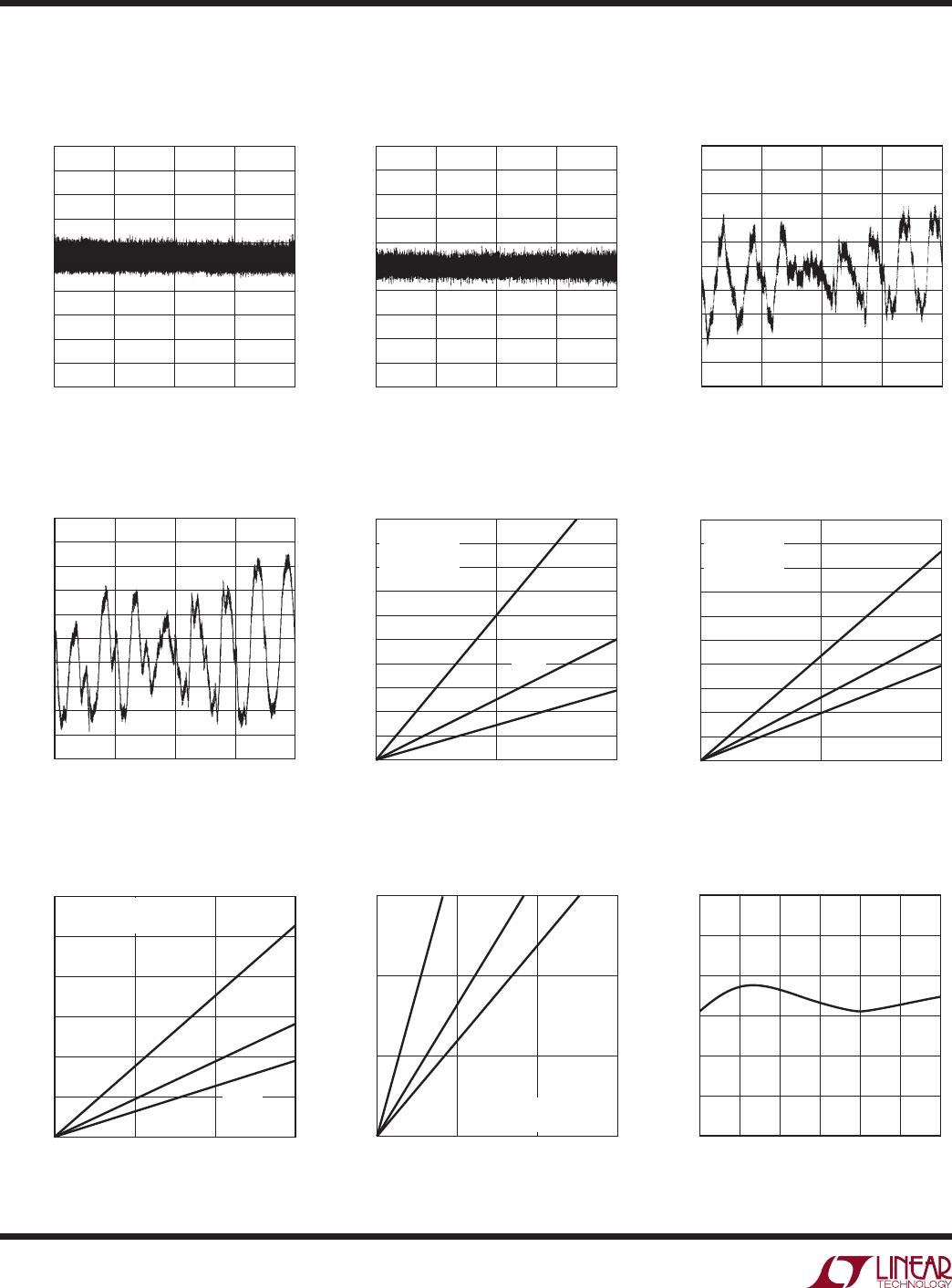
TYPICAL PERFORMANCE CHARACTERISTICS
LTC1657L Integral Nonlinearity
LTC1657 Minimum Supply
Headroom for Full Output Swing
vs Load Current
LTC1657L Minimum Supply
Headroom for Full Output Swing
vs Load Current
LTC1657 Minimum Output
Voltage vs Output Sink Current
LTC1657L Minimum Output
Voltage vs Output Sink Current
LTC1657 Full-Scale Voltage
vs Temperature
LTC1657 Differential Nonlinearity LTC1657L Differential Nonlinearity LTC1657 Integral Nonlinearity
DIGITAL INPUT CODE
0 16384 32768 49152 65535
DIFFERENTIAL NONLINEARITY (LSB)
1657 G01
2.0
1.6
1.2
0.8
0.4
0
0.4
0.8
1.2
1.6
2.0
DIGITAL INPUT CODE
0
2.0
DIFFERENTIAL NONLINEARITY (LSB)
–1.6
0.8
0.4
0
2.0
0.8
16384
32768
49152
1657 G02
–1.2
1.2
1.6
0.4
65535
DIGITAL INPUT CODE
0 16384 32768 49152 65535
INTEGRAL NONLINEARITY (LSB)
1657 G03
5
4
3
2
1
0
1
2
3
4
5
DIGITAL INPUT CODE
0
5
INTEGRAL NONLINEARITY (LSB)
4
2
–1
0
5
2
16384
32768
49152
1657 G04
3
3
4
1
65535
LOAD CURRENT (mA)
0 5 10
V
CC
– V
OUT
(V)
1657 G05
2.0
1.8
1.6
1.4
1.2
1.0
0.8
0.6
0.4
0.2
0
CODE ALL 1s
∆V
OUT
≤ 1LSB
V
OUT
= 4.096V
125°C
25°C
55°C
LOAD CURRENT (mA)
0 5 10
V
CC
– V
OUT
(V)
1657 G06
2.0
1.8
1.6
1.4
1.2
1.0
0.8
0.6
0.4
0.2
0
CODE ALL 1s
∆V
OUT
≤ 1LSB
V
OUT
= 2.5V
125°C
25°C
55°C
OUTPUT SINK CURRENT (mA)
0
5 10 15
OUTPUT PULL-DOWN VOLTAGE (V)
1657 G07
1.2
1.0
0.8
0.6
0.4
0.2
0
CODE ALL 0s
∆V
OUT
≤ 1LSB
125°C
25°C
55°C
OUTPUT SINK CURRENT (mA)
0
5 10 15
OUTPUT PULL-DOWN VOLTAGE (V)
1657 G08
0.6
0.4
0.2
0
CODE ALL 0s
∆V
OUT
≤ 1LSB
125°C 25°C 55°C
TEMPERATURE (°C)
55 25 5 35 65 95 125
FULL-SCALE VOLTAGE (V)
4.110
4.105
4.100
4.095
4.090
4.085
4.080

LTC1657LIGN#TRPBF

Mfr. #:
Manufacturer:
Analog Devices Inc.
Description:
Digital to Analog Converters - DAC Parallel 16-B R2R uP DAC
Lifecycle:
New from this manufacturer.
Delivery:
DHL FedEx Ups TNT EMS
Payment:
T/T Paypal Visa MoneyGram Western Union