LTC1657/LTC1657L
8
1657lfa
For more information www.linear.com/LTC1657
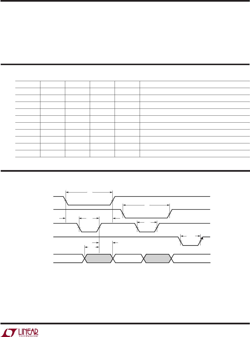
WR (Pin 1): Write Input (Active Low). Used with CSMSB
and/or CSLSB to control the input registers. While WR
and CSMSB and/or CSLSB are held low, data writes into
the input register.
CSLSB (Pin 2): Chip Select Least Significant Byte (Active
Low). Used with WR to control the LSB 8-bit input registers.
While WR and CSLSB are held low, the LSB byte writes
into the
LSB input register. Can be connected to CSMSB
for simultaneous loading of both sets of input latches on
a 16-bit bus.
CSMSB (Pin 3): Chip Select Most Significant Byte (Ac-
tive Low). Used with WR to control the MSB 8-bit input
registers. While WR and CSMSB are held low, the MSB
byte writes into the MSB input register. Can be connected
to CSLSB for simultaneous loading of both
sets of input
latches on a 16-bit bus.
D0 to D7 (Pins 4 to 11): Input data for the Least Significant
Byte. Written into LSB input register when WR = 0 and
CSLSB = 0.
D8 to D15 (Pins 12 to 19): Input data for the Most Signifi-
cant Byte. Written into MSB input register when WR=0
and CSMSB = 0.
GND (Pin 20): Ground.
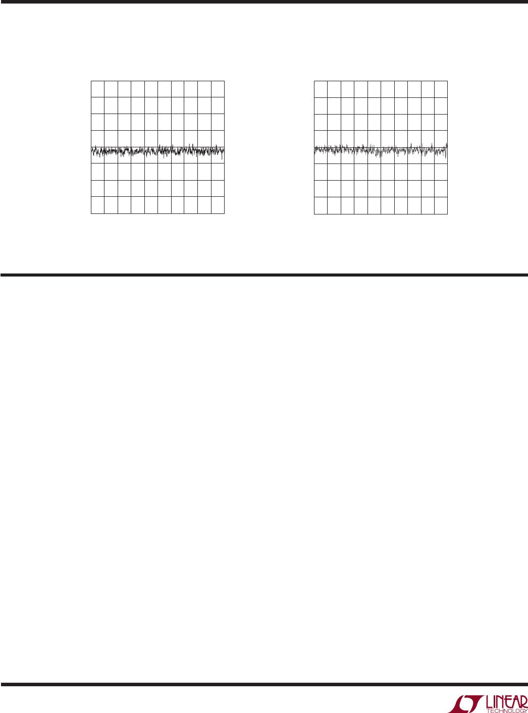
LTC1657 0.1Hz to 10Hz
Voltage Noise
LTC1657L 0.1Hz to 10Hz
Voltage Noise
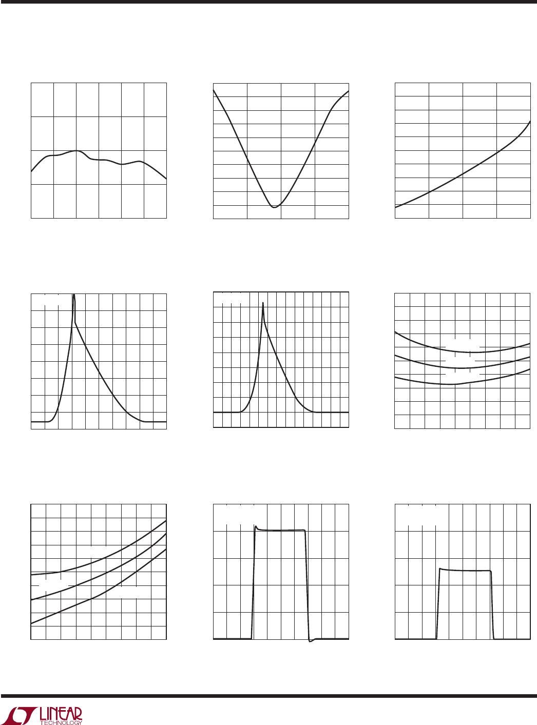
TYPICAL PERFORMANCE CHARACTERISTICS
PIN FUNCTIONS
TIME (SEC)
0
1µV/DIV
8
1659 G19
2 4 6 1071 3 5 9
TIME (SEC)
0
1µV/DIV
8
2 4 6 1071 3 5 9
REFLO (Pin 21): Lower input terminal of the DAC’s internal
resistor ladder. Typically connected to Analog Ground. An
input code of (0000)
H
will connect the positive input of
the output buffer to this end of the ladder. Can be used
to offset the zero scale above ground.
REFHI (Pin 22): Upper input terminal of the DAC’s internal
resistor ladder. Typically connected to REFOUT. An input
code of
(FFFF)
H
will connect the positive input of the output
buffer to 1LSB below this voltage.
REFOUT (Pin 23): Output of the internal reference is 2.048V
(LTC1657), 1.25V (LTC1657L). Typically connected to
REFHI to drive internal DAC resistor ladder.
V
CC
(Pin 24): Positive Power Supply Input. 4.5V ≤ V
CC
≤
5.5V (LTC1657), 2.7V ≤ V
CC
≤ 5.5V (LTC1657L). Requires
a 0.1µF bypass capacitor to ground.
V
OUT
(Pin 25): Buffered DAC Output.
X1/X2 (Pin 26): Gain Setting Resistor Pin. Connect to GND
for G = 2 or to V
OUT
for G = 1. This pin should always be
tied to a low impedance source, such as ground or V
OUT
,
to ensure stability of the output buffer when driving ca-
pacitive loads.