LTC3625/LTC3625-1
4
3625f
Typical perForMance characTerisTics
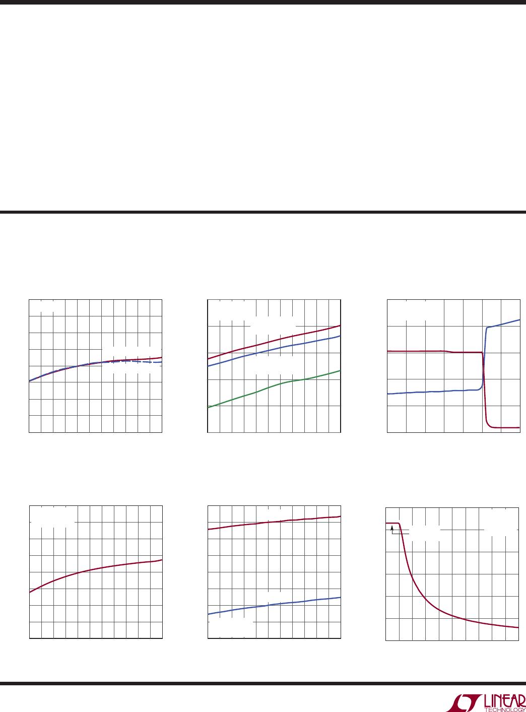
Buck Output Current vs R
PROG
Sleep Current vs V
IN
PROG Voltage and PFI Falling
Threshold vs Temperature
Buck Current Limits
vs Temperature
T
A
= 25°C, L1 = 3.3µH, L2 = 3.3µH, C
IN
= 10µF, C
TOP
= C
BOT
, LTC3625 unless otherwise specified.
elecTrical characTerisTics
Note 1: Stresses beyond those listed under Absolute Maximum Ratings
may cause permanent damage to the device. Exposure to any Absolute
Maximum Rating condition for extended periods may affect device
reliability and lifetime.
Note 2: The LTC3625/LTC3625-1 internal switches are guaranteed to
survive up to 3A of peak current. Internal current limits will restrict peak
current to lower levels.
Note 3: The LTC3625/LTC3625-1 are tested under pulsed load conditions
such that T
J
≈ T
A
. The LTC3625E/LTC3625E-1 are guaranteed to meet
specifications from 0°C to 85°C junction temperature. Specifications over
the –40°C to 125°C operating junction temperature range are assured by
design, characterization and correlation with statistical process controls.
The LTC3625I/LTC3625I-1 are guaranteed over the –40°C to 125°C
operating junction temperature range.
The junction temperature (T
J
in °C) is calculated from the ambient
temperature (T
A
in °C) and power dissipation (P
D
in Watts) according to
the formula:
T
J
= T
A
+ (P
D
θ
JA
)
where θ
JA
(in °C/W) is the package thermal impedance.
Note 4: This IC includes overtemperature protection that is intended to
protect the device during momentary overload conditions. The maximum
rated junction temperature will be exceeded when this protection is active.
Continuous operation above the specified maximum operating junction
temperature may impair device reliability or permanently damage the
device.
Note 5: Measurements are tested with CTL = 0V.
V
IN
(V)
2.7 3.1
0
CURRENT (µA)
10
25
I
VOUT
I
VIN
3.5
4.3
4.7
3625 G01
5
20
15
3.9
5.1
5.5
V
OUT
= 4.8V
V
SEL
= 0V
TEMPERATURE (°C)
–40 –25 –10 5 20 35 50 65 80 95 110
125
V
PROG
(V)
1.205
1.210
1.215
3625 G02
1.195
1.180
1.220
1.200
1.190
1.185
V
IN
= 3.6V
R
PROG
= 143k
Charge Termination Error
vs Temperature
TEMPERATURE (°C)
–40
OFFSET (%)
2.0
1.5
1.0
0.5
0
–0.5
–1.0
–1.5
–2.0
95
3625 G13
5 35 65 12580–10–25 20 50 110
V
IN
= 3.6V
SLEEP THRESHOLD
WAKE THRESHOLD
Input and Output Sleep Currents
vs Temperature
TEMPERATURE (°C)
–40
CURRENT (µA)
25
20
15
10
5
0
95
3625 G14
5 35 65 125
I
VIN
80–10–25 20 50 110
V
IN
= 3.6V
V
SEL
= 3.6V
LTC3625-1 I
VOUT
V
OUT
= 4.5V
LTC3625 I
VOUT
V
OUT
= 5.3V
LTC3625/LTC3625-1
5
3625f
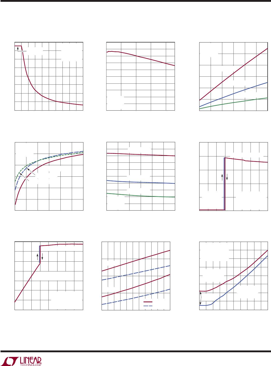
Buck Input Power vs R
PROG
Buck Efficiency vs I
BUCK
R
PROG
(kΩ)
0
INPUT POWER (W)
8
7
6
5
4
3
2
1
0
400
3625 G05
100 200 300 50035050 150 250 450
V
IN
= 5.5V
V
MID
= 2.65V
CTL = 0V
V
SEL
= V
IN
I
PROG
CLAMPED
I
BUCK
(mA)
200
EFFICIENCY (%)
80
90
100
2200
3625 G06
70
60
75
85
95
65
55
50
700
1200
1700
V
IN
= 3.6V
V
MID
= 2V
CTL = 0V
Typical perForMance characTerisTics
T
A
= 25°C, L1 = 3.3µH, L2 = 3.3µH, C
IN
= 10µF, C
TOP
= C
BOT
, LTC3625 unless otherwise specified.
Buck Input Power vs V
MID
V
MID
(V)
0.2
0
INPUT POWER (W)
1
2
3
4
6
0.6
1.0 1.4 1.8
3625 G07
2.2 2.6
5
V
IN
= 5.5V
V
SEL
= V
IN
CTL = 0
R
PROG
= 71.5k
R
PROG
= 143k
R
PROG
= 286k
Buck Efficiency vs V
MID
Buck Output Current vs V
MID
V
MID
(V)
0.2
40
EFFICIENCY (%)
50
60
70
80
100
0.6
1.0 1.4 1.8
3625 G08
2.2 2.6
90
V
IN
= 5.5V
V
SEL
= V
IN
CTL = 0
R
PROG
= 71.5k
R
PROG
= 143k
R
PROG
= 286k
Boost Input Current vs V
TOP
RFET vs TemperatureBoost Efficiency vs V
TOP
V
TOP
(V)
–1.5
EFFICIENCY (%)
60
70
80
1.5
3625 G11
50
40
–0.5 0.5
–1.0 2.0
0 1.0 2.5
30
20
90
V
IN
= 3.6V
V
MID
= 2.5V
V
TOP
= V
OUT
– V
MID
CTL = 0
NORMAL OPERATION
V
OUT
TRICKLE
CHARGE OPERATION
TEMPERATURE (°C)
–40 –25 –10 5 20 35 50 65 80 95 110
125
PMOS R
DS(ON)
(Ω)
NMOS R
DS(ON)
(Ω)
0.15
3625 G12
0
0.20
0.10
0.05
0.20
0.05
0.25
0.15
0.10
V
IN
= 2.7V
V
IN
= 5.5V
PMOS
NMOS
Charge Time vs R
PROG
R
PROG
(kΩ)
0
TIME (SECONDS)
400
350
300
250
200
150
100
50
0
400
3625 G15
100 200 300 50035050 150 250 450
SINGLE
INDUCTOR
APPLICATION
DUAL
INDUCTOR
APPLICATION
V
IN
= 3.6V
V
SEL
= 3.6V
V
OUT
INITIAL = 0V
C
TOP
= C
BOT
= 10F
I
PROG
CLAMPED
LTC3625/LTC3625-1
6
3625f
Typical perForMance characTerisTics
T
A
= 25°C, L1 = 3.3µH, L2 = 3.3µH, C
IN
= 10µF, C
TOP
= C
BOT
, LTC3625 unless otherwise specified.
SW1 (Pin 1): Switch Pin for the Buck Regulator. External
inductor connects between SW1 pin and V
MID
.
V
IN
(Pin 2): Input Voltage Pin. Bypass to GND with a 10µF
or larger ceramic capacitor.
CTL (Pin 3): Logic Input. CTL sets the charge mode of the
LTC3625/LTC3625-1. A logic high at CTL programs the part
to operate with a single inductor; a logic low programs
the part to operate with two inductors. In the 2-inductor
application the capacitor stack will charge approximately
twice as quickly. CTL is a high impedance input and must
be tied to either V
IN
or GND. Do not float.
V
SEL
(Pin 4): Logic Input. V
SEL
selects the output volt-
age of the LTC3625/LTC3625-1. A logic low at V
SEL
sets
the per-cell maximum voltage to 2.45V/2.05V (V
OUT
=
4.8V/4.0V); a logic high sets the per-cell maximum volt-
age to 2.70V/2.30V (V
OUT
= 5.3V/4.5V). When the part is
enabled, V
SEL
has a 4.5MΩ internal pull-down resistor; if
EN is low, then V
SEL
is a high impedance input pin.
EN (Pin 5): Logic Input. Enables the LTC3625/LTC3625-1.
Active high. Has a 4.5MΩ internal pull-down resistor.
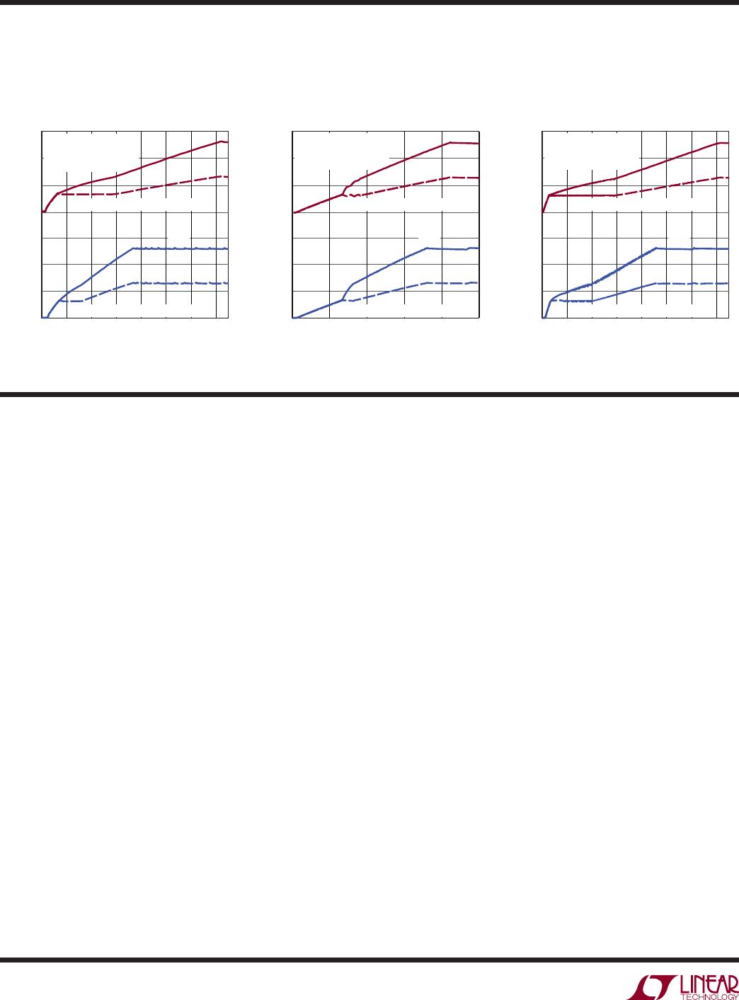
Charge Profile Into Matched
SuperCaps Charge Profile with C
BOT
> C
TOP
Charge Profile with C
TOP
> C
BOT
pin FuncTions
PROG (Pin 6): Charge Current Program Pin. Connecting a
resistor from PROG to ground programs the buck output
current. This pin servos to 1.2V.
PFI (Pin 7): Input to the Power Fail Comparator. This pin
connects to an external resistor divider between V
IN
and
GND. If this functionality is not desired, PFI should be
tied to V
IN
.
PFO (Pin 8): Open-Drain Output of the Power-Fail Compara-
tor. The part pulls this pin low if V
IN
is less than a value
programmed by an external divider. This pin is active low
in shutdown mode. If this functionality is not desired PFO
should be left unconnected.
PGOOD (Pin 9): Logic Output. This is an open-drain
output which indicates that V
OUT
has settled to its final
value. Upon start-up, this pin remains low until the output
voltage, V
OUT
, is within 92.5% (typical) of its final value.
Once V
OUT
is valid, PGOOD becomes high impedance. If
V
OUT
falls to 89.5% (typical) of its correct regulation level,
PGOOD is pulled low. PGOOD may be pulled up through
an external resistor to an appropriate reference level. This
pin is active low in shutdown mode.
TIME (SECONDS)
0
SINGLE INDUCTOR
VOLTAGE (V)
DUAL INDUCTOR
VOLTAGE (V)
0
2
4
120
3625 G16
6
4
20 40 60 80 100 140
2
0
6
V
OUT
V
MID
V
MID
V
IN
= 3.6V, V
SEL
= 3.6V
R
PROG
= 143k
C
TOP
= C
BOT
= 10F
V
OUT
SINGLE INDUCTOR APPLICATION
DUAL INDUCTOR APPLICATION
TIME (SECONDS)
0
SINGLE INDUCTOR
VOLTAGE (V)
DUAL INDUCTOR
VOLTAGE (V)
0
2
4
200
3625 G17
6
4
50 100 150 250
2
0
6
V
OUT
V
MID
V
MID
V
IN
= 3.6V, V
SEL
= 3.6V
R
PROG
= 143k
C
TOP
= 10F, C
BOT
= 50F
V
OUT
SINGLE INDUCTOR APPLICATION
DUAL INDUCTOR APPLICATION
TIME (SECONDS)
0
SINGLE INDUCTOR
VOLTAGE (V)
DUAL INDUCTOR
VOLTAGE (V)
0
2
4
300
3625 G18
6
4
50 100 150 200 250 350
2
0
6
V
OUT
V
MID
V
MID
V
OUT
SINGLE INDUCTOR APPLICATION
DUAL INDUCTOR APPLICATION
V
IN
= 3.6V, V
SEL
= 3.6V
R
PROG
= 143k
C
TOP
= 50F, C
BOT
= 10F
LTC3625IDE#TRPBF

Mfr. #:
Manufacturer:
Analog Devices / Linear Technology
Description:
Battery Management 1A High Efficiency 2-Cell SuperCap Charger with Programmable Charge Current
Lifecycle:
New from this manufacturer.
Delivery:
DHL FedEx Ups TNT EMS
Payment:
T/T Paypal Visa MoneyGram Western Union