LTC3625/LTC3625-1
8
3625f
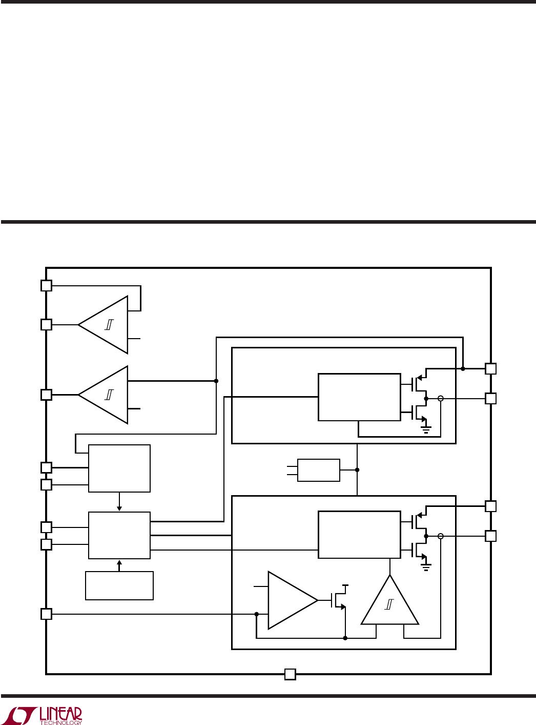
operaTion
The LTC3625/LTC3625-1 are dual cell supercapacitor char-
gers. Their unique topology charges two series connected
capacitors to a fixed output voltage with programmable
charging current without overvoltaging either of the cells
—
even if they are severely mismatched. No balancing
resistors are required. The LTC3625/LTC3625-1 include an
internal buck converter between V
IN
and V
MID
to regulate
the voltage on C
BOT
(across the bottom capacitor) as well
as an internal boost converter between V
MID
and V
OUT
to
regulate the voltage on C
TOP
(across the top capacitor). The
output current of the buck converter is user-programmed
via the PROG pin and the input current of the boost con-
verter is set at 2A (typical).
Table 1 indicates the various functions of the LTC3625/
LTC3625-1 that can be digitally controlled.
Table 1. Digital Input Functions
PIN VALUE FUNCTION
CTL* 0 Part runs in 2-inductor application
1 Part runs in 1-inductor application
V
SEL
0 4.8V/4.0V sleep threshold
1 5.3V/4.5V sleep threshold
EN 0 Part shuts down, V
OUT
becomes high
impedance
1 Part enables and regulates the output
*CTL pin must be hard tied to either V
IN
or GND.
V
IN
Undervoltage Lockout (UVLO)
An internal undervoltage lockout circuit monitors V
IN
and
keeps the LTC3625/LTC3625-1 disabled until V
IN
rises
above 2.90V/2.63V (typical) if V
SEL
is high or 2.63V/2.63V
(typical) if V
SEL
is low. Hysteresis on the UVLO turns off
the LTC3625/LTC3625-1 if V
IN
drops by approximately
100mV below the UVLO rising threshold. When in UVLO,
only current needed to detect a valid input will be drawn
from V
IN
and V
OUT
.
Buck Converter
The buck converter regulates a user-programmed average
output current given by:
I h
V
R
BUCK PROG
PROG
= •
.1 2
where h
PROG
= 118,000 (typical).
The buck converter regulates the current hysteretically by
switching on the buck PMOS until a peak current limit is
reached and then turning on the buck NMOS until a valley
current limit is reached. In the single inductor application
the boost NMOS is used in conjunction with the buck
NMOS to increase efficiency at high currents. The forward
current limit is set to 1.1 • I
BUCK
(typical) and the valley
current limit is set to 0.9 • I
BUCK
(typical). Because of this
method of regulation, overcurrent limit and reverse-current
limit protection is automatically provided. The LTC3625/
LTC3625-1 will continue to regulate its programmed cur-
rent even into a grounded output.
In fault conditions where the PROG pin is shorted to ground,
or R
PROG
is conductive enough to program I
BUCK
to operate
outside of specification, the current out of the PROG pin
will be clamped to 22.5µA (typical) and I
BUCK
will be set to
2.65A (typical). If input current limit is not a concern, the
PROG pin may be grounded to minimize charge times.
Boost Converter
The boost converter regulates a fixed average input current
of 2A (typical). The current is regulated hysteretically by
switching on the boost NMOS until the peak current limit of
2.12A (typical) is reached, and turning on the boost PMOS
until the valley current limit of 1.88A (typical) is reached.
In the single inductor application the buck NMOS is used
in conjunction with the boost NMOS to increase efficiency.
Because of this method of regulation, overcurrent limit and
reverse-current limit protection is automatically provided.
In normal operation V
OUT
will increase with V
MID
so V
OUT
should never be below V
MID
. In the case where there is a
reverse voltage on C
TOP
due to a faulty precondition or a
large load on the output, the boost converter will operate
in trickle charge mode. In this mode the boost PMOS
gate will remain high and instead allow the SW2 node to
increase until SW2 ≈ V
MAX
+ 1V to allow a higher reverse
voltage across the inductor, and the current is ramped down
to 0mA. This will result in a less efficient charge delivery
through the PMOS. To keep dissipation low, I
PEAK
is limited
to 200mA (typical). In this mode the discharge phase is
terminated if it lasts longer than 6.5µs (typical).
The boost converter is disabled if V
MID
falls below the
V
MID(GOOD)
hysteresis threshold of 1.2V (typical).