1
dc2153af
DEMO MANUAL DC2153A
Description
LTC6430-15
300MHz to 1700MHz Differential
ADC Driver/IF/RF Amplifier
Demonstration circuit 2153A features the LTC6430-15
differential ADC/IF Amplifier. The LTC6430-15 has a power
gain of 15.2dB and is part of the LTC6430-YY amplifier
series.
The DC2153A demo board supports the LTC6430-YY ampli
-
fier family
. The DC2153A demo board is optimized for the
frequency
range from 300MHz to 1700MHz and utilizes a
minimum of passive external components to configure the
amplifier for this application. Because The LTC6430-15
L, LT, LTC, LTM, Linear Technology and the Linear logo are registered trademarks of Linear
Technology Corporation. All other trademarks are the property of their respective owners.
has 100Ω differential input and output impedances, so
the demo circuit uses transformers to convert to 50Ω
single-ended so that it can be easily evaluated with most
RF test equipment.
Design files for this circuit board are available at
http://www.
linear.com/demo/DC2153A
Figure 1. LTC6430-15 Device Block Diagram
DC2153a F01
V
CC
9, 22
+IN
BIAS AND TEMPERATURE
COMPENSATION
15dB
GAIN
15dB
GAIN
GND
8, 14, 17, 23 AND PADDLE 25
24
–IN
+OUT
T_DIODE
OUT
7
18
16
13
2
dc2153af
DEMO MANUAL DC2153A
performance summary
Table 1. Typical Demo Board Performance Summary T
A
= 25°C, V
CC
= 5V
SYMBOL PARAMETER CONDITIONS UNITS
Power Supply
V
CC
Operating Supply Range All V
CC
Pins Plus ±OUT 4.75V to 5.25V
I
CC
Current Consumption Total Current 165mA
FREQUENCY
(MHz)
POWER GAIN
|S21| (dB)
OUTPUT
THIRD-ORDER
INTERCEP
T
POINT
(1)
(dBm)
OUTPUT
THIRD-ORDER
INTERMODULATION
POINT
(1)
(dBc)
SECOND
HARMONIC
DISTORTION
(2, 3)
(dBc)
THIRD
HARMONIC
DISTORTION
(2, 3)
(dBc)
OUTPUT 1dB
COMPRESSION
POINT (dBm)
NOISE
FIGURE
(4)
(dB)
300 11.8 41.6 –79.1 –69.2 –72.4 21.3 4.2
400 12.2 41.9 –79.8 –64.4 –69.3 21.6 4.0
500 12.6 42.1 –80.1 –65.5 –71.6 22.2 4.2
600 12.8 43.6 –83.1 –64.9 –68.7 22.3 4.5
700 13.0 45.0 –86.1 –65.3 –71.5 22.6 4.7
800 13.0 47.2 –90.4 –60.8 –73.1 22.4 4.8
900 12.9 46.8 –89.6 –59.1 –77.1 22.0 4.8
1000 12.8 47.1 –90.2 –58.6 –71.7 21.6 5.1
1100 12.7 46.2 –88.4 –57.9 –67.1 21.6 5.3
1200 12.5 45.6 –87.2 –56.2 –65.6 21.4 5.7
1300 12.4 43.7 –83.3 –56.6 –65.3 21.1 5.9
1400 12.3 43.3 –82.6 –66.7 –63.9 20.8 6.2
1500 12.1 40.0 –76.1 –60.5 –62.2 20.4 6.4
1600 11.9 37.2 –70.3 –56.3 –63.7 20.0 6.6
1700 11.6 34.9 –65.9 –56.1 –66.7 19.7 6.8
Notes: All figures are referenced to J1 (Input Port) and J4 (Output Port).
1. Tw o -tone test conditions: Output power level = 2dBm/tone, tone spacing = 1MHz.
2. Single-tone test conditions: Output power level = 6dBm.
3. Degraded performance results are due to imbalance from the balun transformers.
4. Small signal noise figure.
Figure 2. Demo Board S-Parameters
FREQUENCY (MHz)
0
|S21| (dB)
18
16
12
6
4
14
10
8
2
0
|S11|, |S12|, |S22|, (dB)
0
–4
–12
–24
–28
–8
–16
–20
–32
–36
800 1600
DC2153a F02
2000400 1200
|S21|
|S12|
|S11|
|S22|
3
dc2153af
DEMO MANUAL DC2153A
operation
Demo circuit 2153A is a high linearity, fixed gain amplifier.
It is designed for ease of use. The LTC6430-15 is internally
matched to 100Ω differential source and load impedances
from 20MHz to 1400MHz. Due to the unpopularity of
100Ω differential test equipment, transformers have been
added to convert these impedances to single-ended 50Ω.
The frequency range of the circuit is limited by the balun
transformers. Hence, this demo board optimizes the ampli
-
fier per
formance over the frequency range from 300MHz
to
1700MHz. Figure 2 shows the two port DC2153A’s
S-parameters.
The demo circuit’s schematic shows a minimum require
-
ment of passive
support components. Due to the imbalance
from the input and output transformers, the harmonic
distortion performance is slightly degraded. The shunt
capacitors (C8, C9, C25 and C6) help to balance the input
and output signals.
The input and output DC blocking capacitors (C5, C7, C10
and C12) are required because this device is internally
DC-biased for optimal operation. The frequency appropri
-
ate RF
chokes (L2 and L3) and the decoupling capacitors
(C2,
C3, C15 and C16) provide the proper DC bias to the
RF ±OUT ports. A single 5V supply is required for the V
CC
pins on the device.
L1, L4, C6 and C13 are optional components. They are for
additional matching when further optimization to a lower
or wider frequency range applications is required.
A pair of stability networks have been added. They consist
of a 62pF capacitor (C4 and C11) and 348Ω resistor (R1
and R5) in parallel at the LTC6430-15 input network to
ensure low frequency stability.
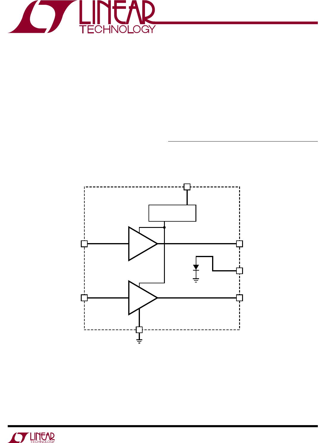
The T_DIODE pin (Turret E1) can be forward biased to
ground with 1mA of current. The measured voltage will
be an indicator of the chip junction temperature (T
J
).
There is an optional circuit at the upper section of the
demo board. This extra circuit can be used to calibrate for
the insertion loss of the demo board’s input and output
components.
Please note that a number of DNC pins are connected on
the demo board. These connections are not necessary for
normal operation, however, failure to float these pins may
impair the operation of the device.
Table 2 shows the function of each input and output on
the board.
Table 2. DC2153A Board I/O Descriptions
CONNECTOR FUNCTION
J1 (IN) Single-ended input. Impedance matched to 50Ω.
Drive from a 50Ω network analyzer or signal source.
J4 (OUT) Single-ended output. Impedance matched to 50Ω.
Drives a 50Ω network analyzer or spectrum analyzer.
E1 (T_DIODE) The measured voltage will be an indicator of the chip
junction temperature.
E2 (V
CC
) Positive supply voltage source.
E3 (GND) Supply ground.

DC2153A

Mfr. #:
Manufacturer:
Analog Devices Inc.
Description:
DEMO BOARD ADC DRIVER/IF/RF AMP
Lifecycle:
New from this manufacturer.
Delivery:
DHL FedEx Ups TNT EMS
Payment:
T/T Paypal Visa MoneyGram Western Union

Products related to this Datasheet