4
dc2153af
DEMO MANUAL DC2153A
aDDitional information
As with any RF device, minimizing ground inductance is
critical. Care should be taken during the board layout when
using these exposed pad packages. A maximum of small-
diameter vias should be placed underneath the exposed
ground pad. This will ensure a good RF ground and low
thermal impedance. Maximizing the copper ground plane
will also improve heat spreading and lower the inductance
to ground. It is a good idea to cover the via holes with
solder mask on the back side of the PCB to prevent solder
from wicking away from the critical PCB to the exposed
pad interface.
The DC2153A is a wide bandwidth demo board, but it is not
intended for operation down to DC. The lower frequency
cutoff is limited by on-chip matching elements.
Table 3 shows the LTC643X-YY amplifier series and its
associated demo boards. Each demo board lists the typical
working frequency range and the input and output imped
-
ance of the amplifiers.
Setup
Signal Sources and Spectrum Analyzer
The
LTC6430-15 is an amplifier with high linearity perfor
-
mance. Therefore, the output intermodulation products are
very low. Even using high dynamic range test equipment,
third-order intercept (IP3) measurements can
drive test
setups
to their limits. Consequently, accurate measure-
ment of
IP3 for a low distortion IC such as the LTC6430-15
requires
certain precautions to be observed in the test
setup as well as the testing procedure.
Setup Signal Sources
Figure 3 shows a proposed IP3 test setup. This setup has
low phase noise, good reverse isolation, high dynamic
range, sufficient harmonic filtering and wideband imped
-
ance matching. The setup is outlined below:
a.
High performance signal generators one and two
(HP8644A) are used. These suggested generators have
low harmonic distortion and very low phase noise.
b. High linearity amplifiers are used to improve the reverse
isolation. This prevents cross talk between the two signal
generators and provides higher output power.
c. A low pass filter is used to suppress the harmonic content
from interfering with the test signal. Note that second
order inputs can mix with the fundamental frequency
to form intermodulation (IM) products of their own. We
suggest filtering the harmonics to –50dBc or better.
d. The signal combiner from mini-circuits (ADP-2-9)
combines the two isolated input signals. This combiner
has a typical isolation of 27dB. For improved VSWR and
isolation, the H-9 signal combiner from
MA/COM is an
alternative which features >40dB isolation and a wider
frequency range. Passive devices (e.g. combiners) with
magnetic elements can contribute nonlinearity to the
signal chain and should be used cautiously.
e. The attenuator pads on all three ports of the signal
combiner will further support isolation of the two input
signal sources. They also reduce reflections and promote
maximum power transfer with wideband impedance
matching.
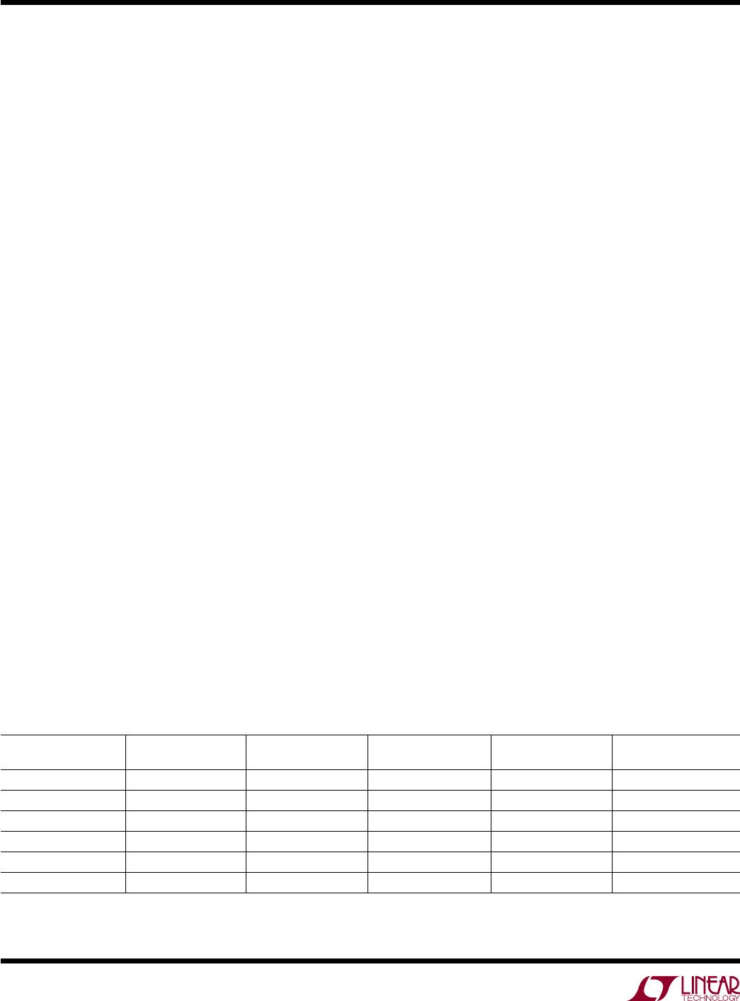
Table 3. The LTC643X-YY Amplifier Family and Corresponding Application Demo Boards
DEMO BOARD
NUMBER
FREQUENCY RANGE
(MHz)
NOTES/
APPLICA
TIONS
BOARD’S IN/OUT
IMPEDANCE
AMPLIFIER AMPLIFIER’S
IMPEDANCE
DC1774A-A 50 to 350 Low Frequency 50Ω LTC6430-15 Differential 100Ω
DC1774A-B 400 to 1000 Mid Frequency 50Ω LTC6430-15 Differential 100Ω
DC1774A-C 100 to 1200 Wide Frequency 50Ω LTC6431-15 Single-Ended 50Ω
DC2032A 50 to 1000 Cable Infrastructure 75Ω LTC6430-15 Differential 100Ω
DC2077A 100 to 1200 Wide Frequency 50Ω LTC6431-20 Single-Ended 50Ω
DC2153A 300 to 1700 High Frequency 50Ω LTC6430-15 Differential 100Ω