XR33181ESBTR

3V to 5.5V, 52Mbps, TSOT23 RS-485/RS-422
Receivers with ±15kV ESD Protection
XR33180/81/83/84
1/12
REV1B
FEATURES
Max 52Mbps data rate
Wide 3.0V to 5.5V supply operation
Robust Electrostatic Discharge (ESD)
protection for RS-485 bus pins
±15kV human body model
±15kV IEC61000-4-2 air discharge
±8kV IEC61000-4-2 contact
discharge
Enhanced receiver failsafe protection for
open, shorted, or terminated but idle data
lines
-40°C to 125°C ambient operating
temperature range
Lead-free (RoHS 6) TSOT23-5 and
TSOT23-6 packaging
Absolute minimum pin count option,
XR33180 (5-pin TSOT23)
Tri-state RO options, XR33181 and
XR33183
Adjustable I/O supply option to help
interfacing to lower voltage logic, XR33184
APPLICATIONS
Clock distribution
Robotic control
Space constrained systems
Security camera networks
Industrial and process control equipment
Description
The XR33180, XR33181, XR33183 and XR33184 are high performance
RS-485/RS-422 receivers designed to meet the increasing system
requirements found in today’s high performance serial communication
applications.
The receiver includes enhanced failsafe circuitry, guaranteeing
a logic-high receiver output when the receiver inputs are open,
shorted, or undriven. The XR33180/81/83/84 (XR3318x) receiver
input impedance is at least 48kΩ (1/4 unit load), allowing more than
128 devices on the bus. The bus pins are ESD protected and pass
IEC61000 level 4 (±15kV).
This is a wide supply (3.0V to 5.5V) device that operates at a maximum
data rate of 52Mbps and comes in very small 5-pin and 6-pin TSOT23
packages, making this standalone receiver ideal for high speed
point-to-point RS-485 applications where space is a concern.
The XR3318x offers several pinout options to maximize performance
in different applications while maintaining a minimum pin count. The
XR33180 is available in a 5-pin TSOT23 package with the receiver
always enabled. The XR33181 is available in a 6-pin TSOT23 package
and offers a active high receiver enable pin while the XR33183 has the
same pinout but with active low enable pin. The XR33184 is available
in a 6-pin TSOT23 package with a I/O logic supply pin to ease the
interface to MCU’s or FPGA’s that run off of different supply voltages.
The V
L
supply pin allows the XR33184 to interface to other devices
running off of supplies from ranging from 1.65V to V
CC
.
All XR3318x options operate up to a max data rate of 52Mbps, and
have excellent propagation delay and skew characteristics making
them a good choice for clock fanout or clock distribution systems.
Typical Application
Figure 1. Typical Application
V
CC
3.3V to 5.0V
RO
120Ω
GND
R
A
B
XR3318x
V
CC
3.3V
GND
D
XR3319x
XR33180/81/83/84
2/12
REV1B
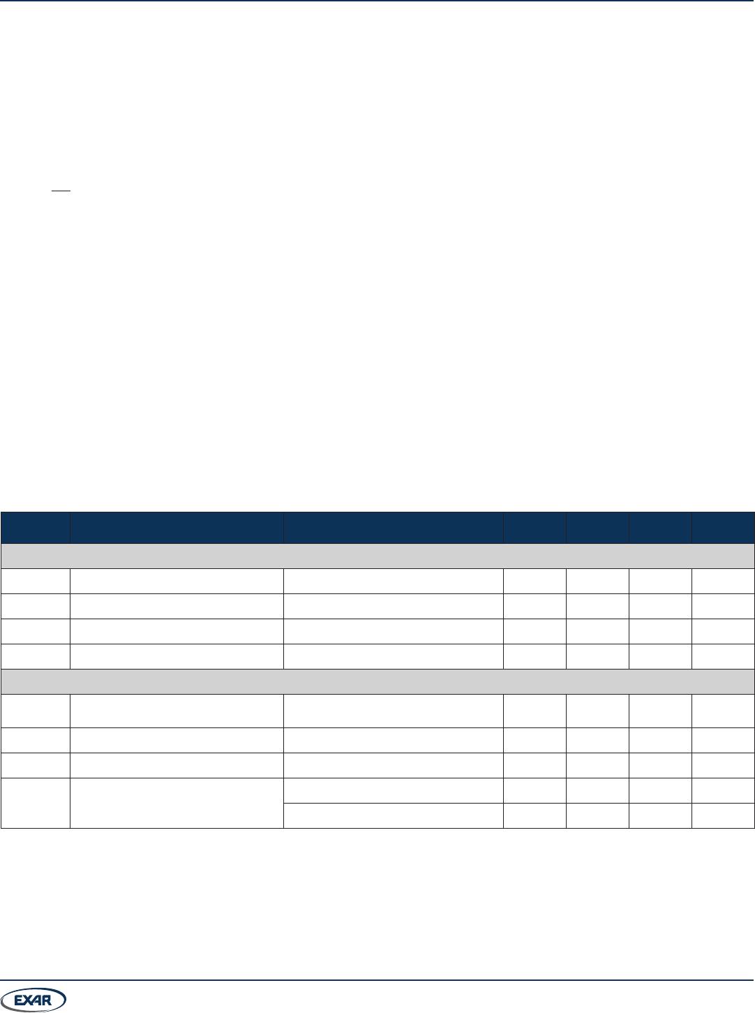
Absolute Maximum Ratings
Stresses beyond those listed under Absolute Maximum
Ratings may cause permanent damage to the device.
Exposure to any Maximum Rating condition for extended
periods may affect device reliability and lifetime.
Supply voltage (V
CC
) ...................................... -0.3V to 7.0V
Junction temperature ................................................. 150°C
Input Voltages
EN and EN ...................................................... -0.3V to 7.0V
Output Voltage
RO (XR33180/81/83) ......................... -0.3V to (V
CC
+ 0.3V)
RO (XR33184) ......................................-0.3V to (V
L
+ 0.3V)
Receiver Input Voltages
A, B ..............................................................................±18V
Transient voltage pulse, through 100Ω
(1)
.................. ±100V
NOTE:
1. Refer to Figure 3.
Operating Conditions
Operating temperature range ...................... -40°C to 125°C
V
CC
supply range .............................................3.0V to 5.5V
Thermal Information
5-pin TSOT23 θ
JA
............................................... 185.5°C/W
5-pin TSOT23 θ
JC
................................................ 61.6°C/W
6-pin TSOT23 θ
JA
............................................... 167.3°C/W
6-pin TSOT23 θ
JC
................................................ 61.6°C/W
Electrical Characteristics
Specifications are at T
A
= 25°C, V
CC
= 3.0V to 5.5V unless otherwise noted. Typical values represent the most likely
parametric norm at T
A
= 25°C, and are provided for reference purposes only.
Symbol Parameter Conditions Min Typ Max Units
Supply
V
CC
Supply voltage range 3.0 5.5 V
V
L
I/O supply voltage range V
L
≤ V
CC
1.65 V
CC
V
I
CC
Supply current No Load, XR33180/81/83/84 2.5 5 mA
I
L
I/O supply No Load, XR33184 10 μA
Receiver DC Characteristics
V
TH
Receiver differential threshold voltage,
V
A
- V
B
-7V ≤ V
CM
≤ 12V -200 -125 -50 mV
∆V
OH
Receiver input hysteresis V
CM
= 0V 25 mV
R
IN
Receiver input resistance -7V ≤ V
CM
≤ 12V 48
I
A,B
Input current, A and B
V
OUT
= 12V, V
CC
= 0V or 5.5V 250 μA
V
OUT
= -7V, V
CC
= 0V or 5.5V -200 μA
XR33180/81/83/84
3/12
REV1B
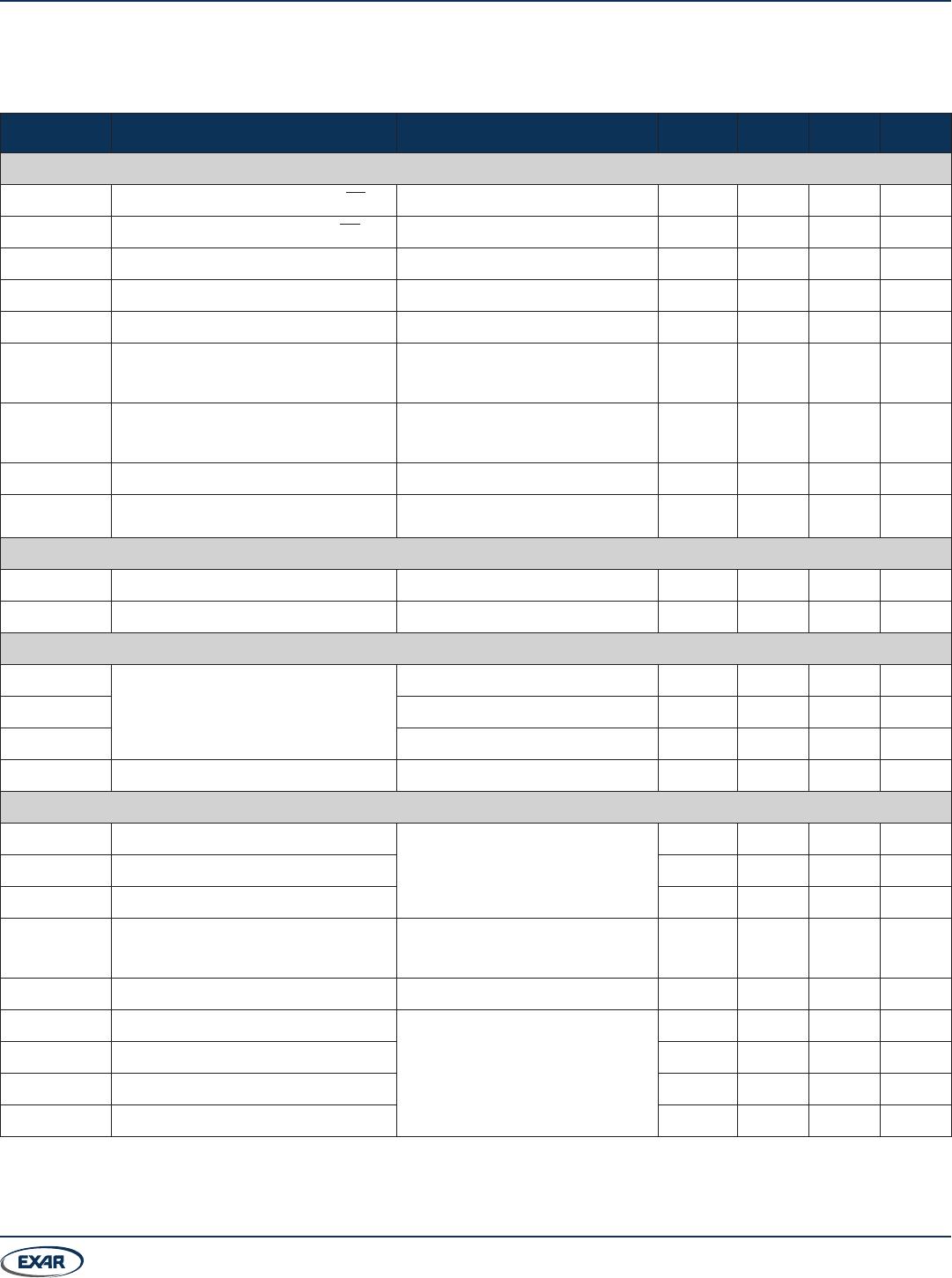
Electrical Characteristics
Specifications are at T
A
= 25°C, V
CC
= 3.0V to 5.5V unless otherwise noted. Typical values represent the most likely
parametric norm at T
A
= 25°C, and are provided for reference purposes only.
Symbol Parameter Conditions Min Typ Max Units
Logic Inputs/Outputs
V
IH
Logic high input thresholds, EN and EN XR33181/83 2 V
V
IL
Logic low input thresholds, EN and EN XR33181/83 0.4 V
I
ENLEAK
Enable pin leakage XR33181/83 -10 10 μA
V
OH
Receiver output high voltage, RO I
OUT
= -4mA, XR33180/81/83 V
CC
- 0.4 V
V
OL
Receiver output low voltage, RO I
OUT
= 4mA, XR33180/81/83 0.4 V
V
OH
Receiver output high voltage, RO
3.0V ≤ V
L
≤ 5.5V, I
OUT
= -4mA
1.65V ≤ V
L
≤ 3.0V, I
OUT
= -1mA,
XR33184
V
L
- 0.4 V
V
OL
Receiver output low voltage, RO
3.0V ≤ V
L
≤ 5.5V, I
OUT
= 4mA
1.65V ≤ V
L
≤ 3.0V, I
OUT
= 1mA,
XR33184
0.4 V
I
OSC
Receiver output short-circuit current 0V ≤ V
RO
≤ V
L
-120 120 mA
I
OZR
High-Z receiver output current
0V ≤ V
OUT
≤ V
CC
, XR33180/81/83
0V ≤ V
OUT
≤ V
L
, XR33184
-1 1 μA
Thermal Characteristics
T
TS
Thermal shutdown temperature 168 °C
T
TSH
Thermal shutdown hysteresis 15 °C
ESD Protection
ESD protection for RS-485 bus pins,
A and B
Human Body Model (HBM) ±15 kV
IEC 61000-4-2 air gap ±15 kV
IEC 61000-4-2 contact ±8 kV
ESD Protection for all other pins Human Body Model (HBM) ±4 kV
Receiver AC Characteristics
t
RPLH
Receiver propagation delay, low to high
C
L
= 15pF, V
ID
= ±2V, V
ID
rise and fall
times <15ns, Figure 4
15 ns
t
RPHL
Receiver propagation delay, high to low 15 ns
|t
RPLH
- t
RPHL
| Receiver propagation delay skew 2 ns
Propagation delay matching, device to
device
(1)
Part to part comparisons must have
the same supply conditions and
temperature difference ≤ 30°C (max)
8 ns
Maximum data rate
(1)
C
L
= 15pF, Duty Cycle 40 to 60% 52 Mbps
t
RZH
Receiver enable to output high
C
L
= 15pF, R
L
= 1KΩ, Figure 5
500 ns
t
RZL
Receiver enable to output low 500 ns
t
RHZ
Receiver disable from output high 500 ns
t
RLZ
Receiver disable from output low 500 ns
NOTE:
1. Guarenteed by design.

XR33181ESBTR

Mfr. #:
Manufacturer:
MaxLinear
Description:
RS-422/RS-485 Interface IC 3V-5.5V Receiver ESD Protection
Lifecycle:
New from this manufacturer.
Delivery:
DHL FedEx Ups TNT EMS
Payment:
T/T Paypal Visa MoneyGram Western Union