XR33180/81/83/84
4/12
REV1B
Pin Configuration
Pin Functions
Pin Number
Pin Name Type Description
XR33180 XR33181 XR33183 XR33184
1 1 1 1 VCC Supply Power supply, bypass with 0.1μf capacitor
2 2 2 2 GND Supply Ground
3 3 3 3 RO Output
Receiver output:
if (V
A
-V
B
) ≥ -50mV, RO is high
if (V
A
-V
B
) ≤ -200mV, RO is low
4 4 4 4 B Bus Input ±15KV ESD protected, RS-485/RS-422 inverting receiver input
- 5 - - EN Input
Receiver output enable:
when EN is low, RO is disabled, high impedance
when EN is high, RO is enabled
- - 5 - EN Input
Receiver output enable:
when EN is high, RO is disabled, high impedance
when EN is low, RO is enabled
- - - 5 VL Supply Logic interface power supply
5 6 6 6 A Bus Input
±15KV ESD protected, RS-485/RS-422 non-inverting receiver
input
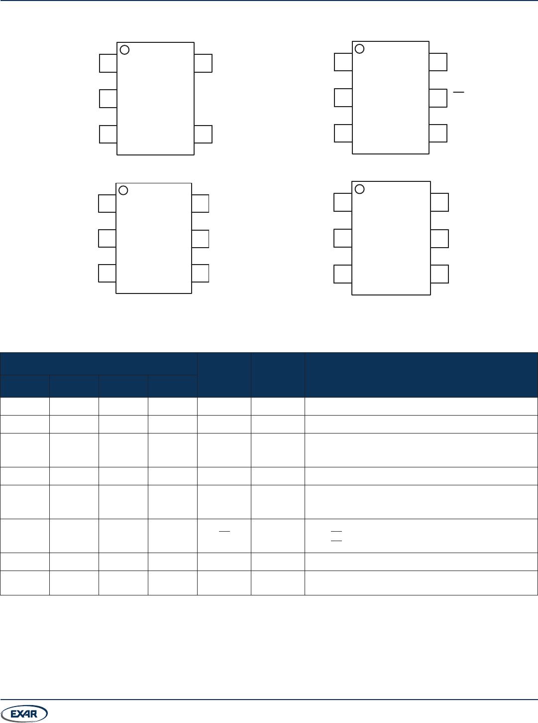
RO
B
A
GND
1
2
5
XR33180
TSOT23-5
VCC
4
3
RO
B
A
GND
1
2
6
XR33181
TSOT23-6
VCC
4
3
EN
5
RO
B
A
GND
1
2
6
XR33183
TSOT23-6
VCC
4
3
EN
5
RO
B
A
GND
1
2
6
XR33184
TSOT23-6
VCC
4
3
VL
5