CAT25080, CAT25160
www.onsemi.com
11
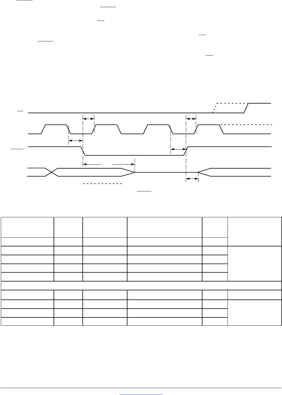
Hold Operation
The HOLD input can be used to pause communication
between host and CAT25080/160. To pause, HOLD
must be
taken low while SCK is low (Figure 11). During the hold
condition the device must remain selected (CS
low). During
the pause, the data output pin (SO) is tri−stated (high
impedance) and SI transitions are ignored. To resume
communication, HOLD
must be taken high while SCK is low.
Design Considerations
The CAT25080/160 devices incorporate Power−On Reset
(POR) circuitry which protects the internal logic against
powering up in the wrong state. The device will power up
into Standby mode after V
CC
exceeds the POR trigger level
and will power down into Reset mode when V
CC
drops
below the POR trigger level. This bi−directional POR
behavior protects the device against ‘brown−out’ failure
following a temporary loss of power.
The CAT25080/160 device powers up in a write disable
state and in a low power standby mode. A WREN instruction
must be issued prior to any writes to the device.
After power up, the CS
pin must be brought low to enter
a ready state and receive an instruction. After a successful
byte/page write or status register write, the device goes into
a write disable mode. The CS
input must be set high after the
proper number of clock cycles to start the internal write
cycle. Access to the memory array during an internal write
cycle is ignored and programming is continued. Any invalid
op−code will be ignored and the serial output pin (SO) will
remain in the high impedance state.
Figure 11. HOLD Timing
SCK
SO
HIGH IMPEDANCE
Dashed Line = mode (1, 1)
t
LZ
CS
HOLD
t
CD
t
HD
t
HD
t
CD
t
HZ
ORDERING INFORMATION (Notes 13 − 16)
Device Order
Number
Specific
Device
Marking*
Package Type Temperature Range
Lead
Finish
Shipping
†
CAT25080HU4I-GT3 S3U UDFN8−EP I = Industrial (−40°C to +85°C) NiPdAu
CAT25080VI-GT3 25080D SOIC−8, JEDEC I = Industrial (−40°C to +85°C) NiPdAu
Tape & Reel,
3,000 Units / Reel
CAT25080VE-GT3 25080D SOIC−8, JEDEC E = Extended (−40°C to +125°C) NiPdAu
CAT25080YI-GT3 S08D TSSOP−8 I = Industrial (−40°C to +85°C) NiPdAu
CAT25080YE-GT3 S08D TSSOP−8 E = Extended (−40°C to +125°C) NiPdAu
CAT25160HU4I-GT3 S4U UDFN8−EP I = Industrial (−40°C to +85°C) NiPdAu
CAT25160VI-GT3 25160D SOIC−8, JEDEC I = Industrial (−40°C to +85°C) NiPdAu
Tape & Reel,
3,000 Units / Reel
CAT25160VE-GT3 25160D SOIC−8, JEDEC E = Extended (−40°C to +125°C) NiPdAu
CAT25160YI-GT3 S16D TSSOP−8 I = Industrial (−40°C to +85°C) NiPdAu
†For information on tape and reel specifications, including part orientation and tape sizes, please refer to our Tape and Reel Packaging
Specifications Brochure, BRD8011/D.
13.All packages are RoHS−compliant (Lead−free, Halogen−free).
14.The standard lead finish is NiPdAu.
15.For detailed information and a breakdown of device nomenclature and numbering systems, please see the ON Semiconductor Device
Nomenclature document, TND310/D, available at www.onsemi.com
16.For additional package and temperature options, please contact your nearest ON Semiconductor Sales office.
17.Not recommended for new design