CAT25080, CAT25160
www.onsemi.com
5
Pin Description
SI: The serial data input pin accepts op−codes, addresses
and data. In SPI modes (0,0) and (1,1) input data is latched
on the rising edge of the SCK clock input.
SO: The serial data output pin is used to transfer data out of
the device. In SPI modes (0,0) and (1,1) data is shifted out
on the falling edge of the SCK clock.
SCK: The serial clock input pin accepts the clock provided
by the host and used for synchronizing communication
between host and CAT25080/160.
CS
: The chip select input pin is used to enable/disable the
CAT25080/160. When CS
is high, the SO output is tri−stated
(high impedance) and the device is in Standby Mode (unless
an internal write operation is in progress). Every
communication session between host and CAT25080/160
must be preceded by a high to low transition and concluded
with a low to high transition of the CS
input.
WP
: The write protect input pin will allow all write
operations to the device when held high. When WP
pin is
tied low and the WPEN bit in the Status Register (refer to
Status Register description, later in this Data Sheet) is set to
“1”, writing to the Status Register is disabled.
HOLD
: The HOLD input pin is used to pause transmission
between host and CAT25080/160, without having to
retransmit the entire sequence at a later time. To pause,
HOLD
must be taken low and to resume it must be taken
back high, with the SCK input low during both transitions.
When not used for pausing, the HOLD input should be tied
to V
CC
, either directly or through a resistor.
Functional Description
The CAT25080/160 devices support the Serial Peripheral
Interface (SPI) bus protocol, modes (0,0) and (1,1). The
device contains an 8−bit instruction register. The instruction
set and associated op−codes are listed in Table 9.
Reading data stored in the CAT25080/160 is
accomplished by simply providing the READ command and
an address. Writing to the CAT25080/160, in addition to a
WRITE command, address and data, also requires enabling
the device for writing by first setting certain bits in a Status
Register, as will be explained later.
After a high to low transition on the CS
input pin, the
CAT25080/160 will accept any one of the six instruction
op−codes listed in Table 9 and will ignore all other possible
8−bit combinations. The communication protocol follows
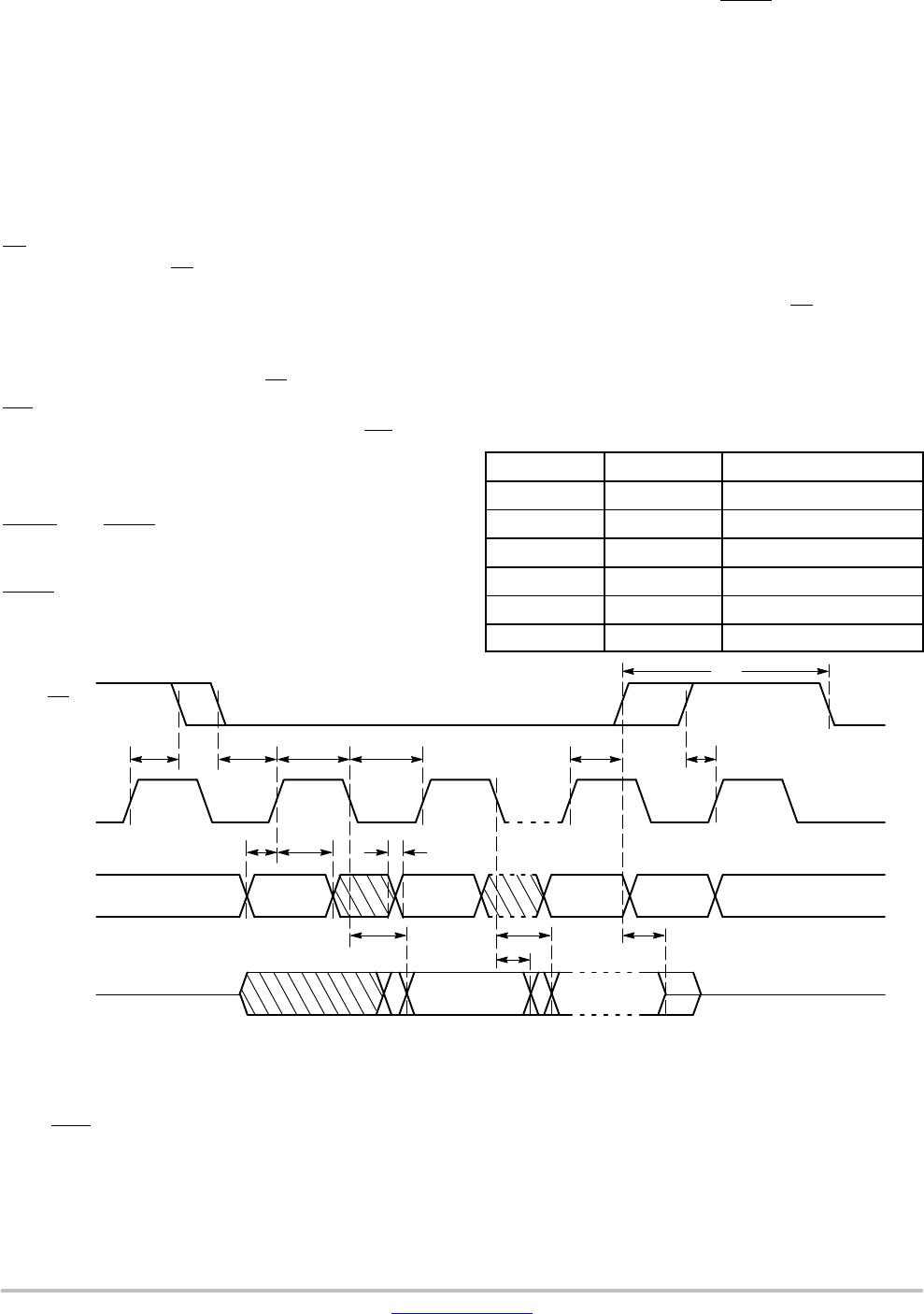
the timing from Figure 2.
Table 9. INSTRUCTION SET
Instruction Opcode Operation
WREN 0000 0110 Enable Write Operations
WRDI 0000 0100 Disable Write Operations
RDSR 0000 0101 Read Status Register
WRSR 0000 0001 Write Status Register
READ 0000 0011 Read Data from Memory
WRITE 0000 0010 Write Data to Memory
Figure 2. Synchronous Data Timing
CS
SCK
SI
SO
t
CNH
t
CSS
t
WH
t
WL
t
SU
t
H
HI−Z
VALID
IN
VALID
OUT
t
CSH
t
RI
t
FI
t
V
t
V
t
HO
t
CNS
t
CS
HI−Z
t
DIS
Status Register
The Status Register, as shown in Table 10, contains a
number of status and control bits.
The RDY
(Ready) bit indicates whether the device is busy
with a write operation. This bit is automatically set to 1 during
an internal write cycle, and reset to 0 when the device is ready
to accept commands. For the host, this bit is read only.
The WEL (Write Enable Latch) bit is set/reset by the
WREN/WRDI commands. When set to 1, the device is in a
Write Enable state and when set to 0, the device is in a Write
Disable state.
The BP0 and BP1 (Block Protect) bits determine which
blocks are currently write protected. They are set by the user
with the WRSR command and are non−volatile. The user is
allowed to protect a quarter, one half or the entire memory,
by setting these bits according to Table 11. The protected
blocks then become read−only.