Integrated Silicon Solution, Inc. — www.issi.com —
1-800-379-4774
1
Rev. B
06/08/05
ISSI
®
Copyright © 2005 Integrated Silicon Solution, Inc. All rights reserved. ISSI reserves the right to make changes to this specification and its products at any time without notice. ISSI assumes no liability
arising out of the application or use of any information, products or services described herein. Customers are advised to obtain the latest version of this device specification before relying on any
published information and before placing orders for products.
IS61C6416AL IS64C6416AL
IS62C6416AL IS65C6416AL
FEATURES
IS61C6416AL and IS64C6416AL
• High-speed access time: 12 ns, 15ns
• Low Active Power: 175 mW (typical)
• Low Standby Power: 1 mW (typical)
CMOS standby
IS62C6416AL and IS65C6416AL
• High-speed access time: 35 ns, 45ns
• Low Active Power: 50 mW (typical)
• Low Standby Power: 100 µW (typical)
CMOS standby
• TTL compatible interface levels
• Single 5V ± 10% power supply
• Fully static operation: no clock or refresh
required
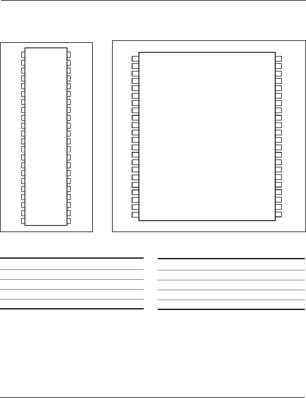
• Available in 44-pin SOJ package and
44-pin TSOP (Type II)
• Commercial, Industrial and Automotive tempera-
ture ranges available
• Lead-free available
DESCRIPTION
The ISSI IS61C6416AL, IS62C6416AL, IS64C6416AL and
IS65C6416AL are high-speed, 1,048,576-bit static RAMs
organized as 65,536 words by 16 bits. They are fabricated
using ISSI's high-performance CMOS technology. This highly
reliable process coupled with innovative circuit design tech-
niques, yields access times as fast as 12 ns with low power
consumption.
When CE is HIGH (deselected), the device assumes a
standby mode at which the power dissipation can be reduced
down with CMOS input levels.
Easy memory expansion is provided by using Chip Enable
and Output Enable inputs, CE and OE. The active LOW Write
Enable (WE) controls both writing and reading of the memory.
A data byte allows Upper Byte (UB) and Lower Byte (LB)
access.
The IS61C6416AL, IS62C6416AL, IS64C6416AL and
IS65C6416AL are packaged in the JEDEC standard 44-pin
400-mil SOJ and 44-pin TSOP (Type II).
FUNCTIONAL BLOCK DIAGRAM
JUNE 2005
A0-A15
CE
OE
WE
64K x 16
MEMORY ARRAY
DECODER
COLUMN I/O
CONTROL
CIRCUIT
GND
VDD
I/O
DATA
CIRCUIT
I/O0-I/O7
Lower Byte
I/O8-I/O15
Upper Byte
UB
LB
64K x 16 HIGH-SPEED CMOS STATIC RAM