81006 DATA SHEET
VCXO-TO-6 LVCMOS OUTPUTS 2 REVISION B 7/29/16
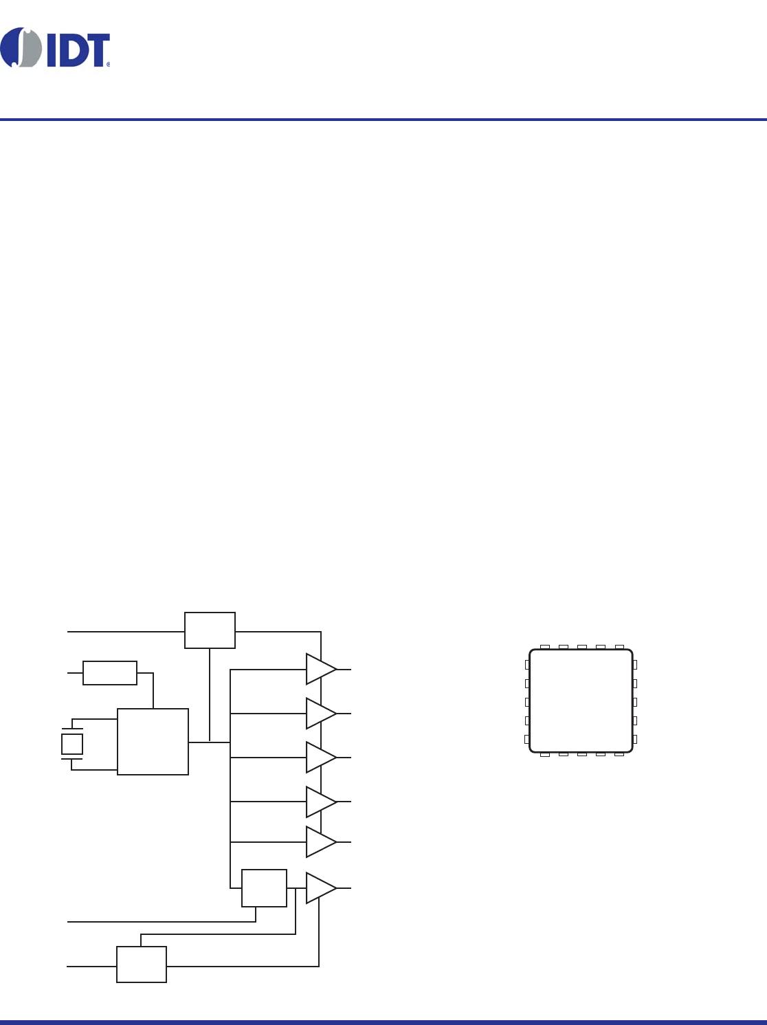
Pin Descriptions and Characteristics
Table 1. Pin Descriptions
1
Number Name Type
1, 2
XTAL_IN,
XTAL_OUT
Input Crystal oscillator interface. XTAL_IN is th
e input. XTAL_OUT is the output.
3 V
DD
Power Positive supply pin.
4 VC Input Control voltage input.
5 DIV_SEL_Q5 Input Pulldown
Output divider select pin for Q5 output. When LOW, ÷1. When HIGH, ÷2.
LVCMOS/LVTTL in
terface levels.
6 OE1 Input Pullup
Output enable pin. When HIGH, Q5 output is enabled. When LOW, forces
Q5 to a high
impedance state. LVCMOS/LVTTL interface levels.
7, 11, 15, 19 GND Power Power supply ground.
8, 10, 12, 14,
16, 1
8
Q5, Q4, Q3,
Q2, Q1, Q0
Output
Single-ended clock outputs. LVCMOS/LVTTL interface levels. 20ou
tput
impedance.
9, 13, 17 V
DDO
Power Output supply pins.
20 OE0 Input Pullup
Output enable pin. When HIGH, Q0:Q4 outputs are enabled. When LOW,
fo
rces Q0:Q4 to a high impedance state. LVCMOS/LVTTL interface levels.
Description
NOTE 1: Pullup and Pulldown refer to internal input resistors. See Table 2, Pin Characteristics, for typical values.
Table 2. Pin Characteristics
Symbol Parameter Test Conditions Minimum Typical Maximum Units
C
IN
Input
Capacitance
OE0, OE1 4 pF
C
PD
Power Dissipation
Capacitance
V
DD
= V
DDO
= 3.465V 3 pF
V
DD
= 3.465V or 2.625V,
V
DDO
= 2.625V
4pF
V
DD
= 3.465V or 2.625V,
V
DDO
= 2V
6pF
R
PULLUP
Input Pullup Resistor 51 k
R
PULLDOWN
Input Pulldown Resistor 51 k
R
OUT
Output Impedance
V
DDO
= 3.3V 20
V
DDO
= 2.5V 25
V
DDO
= 1.8V 38