81006 DATA SHEET
VCXO-TO-6 LVCMOS OUTPUTS 4 REVISION B 7/29/16
Table 3C. LVCMOS/LVTTL DC Characteristics, T
A
= 0°C to 70°C
Symbol Parameter Test Conditions Minimum Typical Maximum Units
V
IH
Input High Voltage
V
DD
= 3.3V ±5% 2V
DD
+ 0.3 V
V
DD
= 2.5V ±5% 1.7 V
DD
+ 0.3 V
V
IL
Input Low
Voltage
OE0, OE1,
DIV_SEL_Q5
V
DD
= 3.3V ±5% -0.3 0.8 V
V
DD
= 2.5V ±5% -0.3 0.7 V
VC VCXO Control Voltage 0 V
DD
V
I
IH
Input
High Current
DIV_SEL_Q5 V
DD
= 3.3V or 2.5V ±5% 150 µA
OE0, OE1 V
DD
= 3.3V or 2.5V ±5% A
I
IL
Input
Low Current
DIV_SEL_Q5 V
DD
= 3.3V or 2.5V ±5% -5 µA
OE0, OE1 V
DD
= 3.3V or 2.5V ±5% -150 µA
I
I
Input Current of VC pin V
DD
= 3.465V or 2.625V -100 100 µA
V
OH
Output High Voltage
1
V
DDO
= 3.3V ±5% 2.6 V
V
DDO
= 2.5V ±5% 1.8 V
V
DDO
= 1.8V ±0.2V 1.5 V
V
OL
Output Low Voltage
1
V
DDO
= 3.3V or 2.5V ±5% 0.5 V
V
DDO
= 1.8V ±0.2V 0.4 V
NOTE 1: Outputs terminated with 50to V
DDO
/2. See Parameter Measurement Information section, “Load Test Circuit” diagrams.
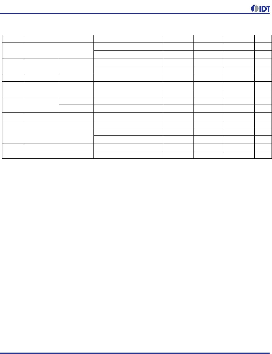
Table 4C. AC Characteristics, V
DD
= 3.3V ±5%, V
DDO
= 1.8V ±0.2V, T
A
= 0°C to 70°C
Test Conditions Minimum Typical Maximum Units
f
OUT
Output Frequency 12 19.44 31.25 MHz
tjit(Ø) RMS Phase Jitter (Random)
1
Integration Range: 1kHz – 1MHz 0.27 ps
tsk(o) Output Skew
2, 3
Q0:Q4 46 ps
Q0:Q5 DIV_SEL_Q5 = ÷1 175 ps
t
R
/ t
F
Output Rise/Fall Time 20% to 80% 450 1400 ps
odc Output Duty Cycle 44 56 %
REVISION B 7/29/16 5 VCXO-TO-6 LVCMOS OUTPUTS
81006 DATA SHEET
AC Characteristics
Table 4A. AC Characteristics, V
DD
= V
DDO
= 3.3V ±5%, T
A
= 0°C to 70°C
Symbol Parameter Test Conditions Minimum Typical Maximum Units
f
OUT
Output Frequency 12 19.44 31.25 MHz
tjit(Ø) RMS Phase Jitter (Random)
1
NOTE 1: Refer to the Phase Noise Plot.
Integration Range: 1kHz – 1MHz 0.35 ps
tsk(o) Output Skew
2, 3
NOTE 2: Defined as skew between outputs at the same supply voltage and with equal load conditions. Measured at the output differential
crosspoints.
NOTE 3: This parameter is defined in accordance with JEDEC Standard 65.
Q0:Q4 30 ps
Q0:Q5 DIV_SEL_Q5 = ÷1 100 ps
t
R
/ t
F
Output Rise/Fall Time 20% to 80% 200 700 ps
odc Output Duty Cycle 44 56 %
Table 4B. AC Characteristics, V
DD
= 3.3V ±5%, V
DDO
= 2.5V ±5%, T
A
= 0°C to 70°C
Symbol Parameter Test Conditions Minimum Typical Maximum Units
f
OUT
Output Frequency 12 19.44 31.25 MHz
tjit(Ø) RMS Phase Jitter (Random)
1
NOTE 1: Refer to the Phase Noise Plot.
Integration Range: 1kHz – 1MHz 0.38 ps
tsk(o) Output Skew
2, 3
NOTE 2: Defined as skew between outputs at the same supply voltage and with equal load conditions. Measured at the output differential
crosspoints.
NOTE 3: This parameter is defined in accordance with JEDEC Standard 65.
Q0:Q4 20 ps
Q0:Q5 DIV_SEL_Q5 = ÷1 90 ps
t
R
/ t
F
Output Rise/Fall Time 20% to 80% 300 800 ps
odc Output Duty Cycle 45 55 %
Symbol Parameter
NOTE 1: Refer to the Phase Noise Plot.
NOTE 2: Defined as skew between outputs at the same supply voltage and with equal load conditions. Measured at the output differential
crosspoints.
NOTE 3: This parameter is defined in accordance with JEDEC Standard 65.
Table 4D. AC Characteristics, V
DD
= V
DDO
= 2.5V ±5%, T
A
= 0°C to 70°C
Test Conditions Minimum Typical Maximum Units
f
OUT
Output Frequency 12 19.44 31.25 MHz
tjit(Ø) RMS Phase Jitter (Random)
1
Integration Range: 1kHz – 1MHz 0.28 ps
tsk(o) Output Skew
2, 3
Q0:Q4 25 ps
Q0:Q5 DIV_SEL_Q5 = ÷1 100 ps
t
R
/ t
F
Output Rise/Fall Time 20% to 80% 300 800 ps
odc Output Duty Cycle 45 55 %
Table 4E. AC Characteristics, V
DD
= 2.5V ±5%, V
DDO
= 1.8V ±0.2V, T
A
= 0°C to 70°C
Test Conditions Minimum Typical Maximum Units
f
OUT
Output Frequency 12 19.44 31.25 MHz
tji
t(Ø) RMS Phase Jitter (Random)
1
Integration Range: 1kHz – 1MHz 0.26 ps
tsk(o) Output Skew
2, 3
Q0:Q4 40 ps
Q0:Q5 DIV_SEL_Q5 = ÷1 175 ps
t
R
/ t
F
Output Rise/Fall Time 20% to 80% 450 1400 ps
odc Output Duty Cycle 40 60 %
81006 DATA SHEET
VCXO-TO-6 LVCMOS OUTPUTS 6 REVISION B 7/29/16
Symbol Parameter
NOTE 1: Refer to the Phase Noise Plot.
NOTE 2: Defined as skew between outputs at the same supply voltage and with equal load conditions. Measured at the output differential
crosspoints.
NOTE 3: This parameter is defined in accordance with JEDEC Standard 65.
Symbol Parameter
NOTE 1: Refer to the Phase Noise Plot.
NOTE 2: Defined as skew between outputs at the same supply voltage and with equal load conditions. Measured at the output differential
crosspoints.
NOTE 3: This parameter is defined in accordance with JEDEC Standard 65.

81006AKLFT

Mfr. #:
Manufacturer:
IDT
Description:
Clock Generators & Support Products 6 CMOS OUT VCXO
Lifecycle:
New from this manufacturer.
Delivery:
DHL FedEx Ups TNT EMS
Payment:
T/T Paypal Visa MoneyGram Western Union

Products related to this Datasheet